
SEMICON Taiwan 2026 was held from September 2 to 4 at Taipei Nangang Exhibition Center Halls 1 and 2, featuring key technologies including AI chips, advanced process technologies, advanced packaging, silicon photonics, quantum computing, and HBM. A central theme of this year’s event was the evolving role of advanced packaging, which has moved beyond traditional back-end manufacturing to become a critical part of system integration. At the same time, as AI computing continues to scale, system performance bottlenecks are shifting away from the computing power of individual chips toward a combination of constraints, including memory bandwidth, chip-to-chip I/O efficiency, and the energy required for data movement. Overall, industry competition is moving beyond simply pursuing faster computing speeds toward improving data transfer efficiency and system integration capabilities.
Customer Base Becomes More Diversified as Solutions to Process Bottlenecks Take Center Stage
Compared with previous years, one of the most notable changes at this year’s event was the increasingly diversified customer base among equipment suppliers. In the past, orders for participating equipment vendors were heavily concentrated among Taiwan’s major foundry customers. This year, however, demand from OSAT providers strengthened significantly, while U.S. IDMs, memory manufacturers, and Taiwanese suppliers associated with the Terafab supply chain in Texas have also reported new progress and equipment qualification activities. This indicates that demand for advanced process and packaging equipment is gradually expanding from a single major customer to a broader range of applications and customers.
Another significant change was the growing focus on solutions addressing real-world manufacturing bottlenecks. Equipment related to warpage control, temperature control, precision alignment, and micro-contamination control was far more prominent than in previous years, with a particularly sharp increase in solutions related to CPO and TGV. As advanced packaging moves toward higher levels of integration, the manufacturing challenges associated with introducing glass materials, together with the stringent precision alignment and process control requirements of optical components, are creating new technical barriers. This gives equipment and process suppliers with relevant capabilities a stronger competitive advantage.
In addition, several equipment suppliers highlighted the adoption of AI agents to optimize design, process tuning, and troubleshooting. Among them, Chunghwa Precision Test Tech’s Agent P intelligent agent system was one of the most comprehensive solutions presented. Supply-demand conditions also showed positive signals, with lead times for some equipment extending from approximately six to nine months to nine to twelve months. Despite recent market concerns over AI chip upgrades or potential specification reductions, there has yet to be a noticeable impact on equipment upgrades or purchasing momentum. This suggests that downstream capital expenditure and demand for advanced process and packaging equipment remain strong.
Advanced Packaging: FOPLP Is Beginning to Gain Traction
FOPLP was one of the most structurally significant developments in advanced packaging at this year’s event. In 2024, mainstream high-end packages were approximately 3.3 times the size of a single reticle limit. This figure is expected to increase to 14 times by 2030 and potentially exceed 20 times. As package sizes continue to expand, the area utilization efficiency of circular wafers declines significantly. By comparison, rectangular panels can achieve utilization rates of more than 95%. FOPLP therefore offers better material utilization for large-format advanced packaging, potentially reducing overall manufacturing costs by approximately 30% to 50% compared with wafer-level solutions.
Further Reading | What Is PLP? How Panel-Level Packaging Is Reshaping the AI Advanced Packaging Market?
Technology and mass-production strategies are now beginning to diverge among manufacturers. ASE Technology Holding (3711.TW) is using a 310mm square panel as its standardized entry point and has completed the development of eight-layer high-density RDL. The company plans to perform front-end processing on large panels before cutting them into four 310mm panels that can be integrated with its existing automated assembly lines. Its process also incorporates slot-die coating and LDI laser direct imaging, significantly improving photoresist utilization efficiency.
Powertech Technology (6239.TW) is using its Clear and Pidal platforms to achieve 1μm line width and spacing, along with high-density RDL featuring a combined total of 10 layers on the top and bottom. It has already delivered AI accelerator products with package areas reaching 5.5 times the reticle size.
Traditional display panel manufacturers are also moving aggressively into the market. Innolux (3481.TW) has begun mass production of automotive RFICs using 700×700mm glass substrates, achieving a 99.5% yield. AUO (2409.TW) , meanwhile, partnered with Corning to demonstrate a copper-plated TGV glass core substrate, with the two companies dividing responsibilities for laser drilling and copper metallization. This demonstrates how existing panel manufacturing capabilities are gradually extending into advanced packaging.

However, FOPLP still faces several critical technical bottlenecks. As panel sizes increase, challenges involving warpage control, airflow uniformity, and electroplating uniformity become significantly more difficult. Glass also has lower thermal conductivity than silicon interposers, increasing the complexity of thermal design for high-power AI chips. According to Yuanta’s estimated timeline, panel-level packaging mass-production lines remain in the qualification stage. Mass-production equipment specifications are expected to be finalized in the second half of 2027, followed by large-scale equipment shipments in the first half of 2028. End products are expected to enter larger-scale mass production between the second half of 2028 and the first half of 2029. This suggests that FOPLP will remain focused primarily on process qualification and equipment investment in the near term, with meaningful large-scale contributions unlikely before 2028.
Silicon Photonics and CPO: Technology Roadmaps Converge as Testing and Optical Alignment Become Key Bottlenecks

CPO was one of the most closely watched technology themes at SEMICON Taiwan this year, driven primarily by the increasingly apparent I/O Wall. TSMC (2330.TW) noted that AI chip computing performance increases by approximately 3 times every two years, while memory bandwidth and chip-to-chip I/O bandwidth grow by only 1.6 times and 1.4 times, respectively. Conventional copper interconnects are gradually approaching their limits for high-frequency, long-distance transmission, accelerating the transition of data transmission architectures from electrical to optical connections.
TSMC is currently using COUPE as its primary technology platform, integrating EIC and PIC through SoIC-X while developing both CPO-MCM and CPO-OOI architectures. ASE is approaching the market from the packaging side, using FOCoS-Bridge to advance the integration of optical engines with computing chips. Overall, industry technology roadmaps are gradually converging around high-density optoelectronic integration and placing optical engines closer to computing chips.
Rather than architecture selection, testing and optical alignment have emerged as the real bottlenecks to CPO mass production. Coupling loss currently needs to be kept below 0.3dB, while manufacturing and assembly processes still typically achieve only 0.5–1dB. Alignment error for detachable fiber arrays must also remain within 0.3 degrees. In addition, dual-sided optoelectronic testing equipment can weigh six to eight metric tons per unit, creating more stringent requirements for facility load-bearing capacity, micro-vibration control, and equipment integration.
Taiwanese equipment suppliers are also accelerating their qualification efforts. Hon. Precision (7769.TW) is developing simultaneous optoelectronic testing for Insertion 4, while MPI (6223.TW) and Hermes Testing (7856.TW) are advancing solutions for Insertion 2 and 3. All Ring Tech (6187.TW) and FitTech (6706.TW) are focusing on FAU coupling and bonding equipment, Msscorps (6830.TW) is moving into dual-sided optoelectronic testing, and E&R Engineering (8027.TW) is using laser processing to reduce FAU manufacturing costs. Overall, the direction of CPO technology is becoming increasingly clear. Whether the industry can ultimately achieve large-scale mass production will depend on the establishment of testing standards, improvements in optical alignment efficiency, and whether equipment suppliers can simultaneously deliver precision, speed, and cost efficiency.
Further Reading | Introduction to the Silicon Photonics Industry & What Is CPO
Memory: From Basic Component to Strategic Resource as Bandwidth, Energy Efficiency, and Architecture Advance
As memory supply remains tight, rising prices have become a clear market trend. Against this backdrop of increasing costs, the central message from this year’s Memory Summit was that memory is evolving from a conventional electronic component into a strategic resource that determines both AI system performance and overall cost.
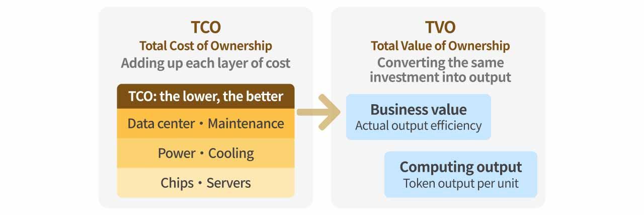
As AI models scale rapidly, GPU computing performance is growing significantly faster than HBM bandwidth, while moving data consumes substantially more energy than the computations themselves. Memory has therefore become a major bottleneck in AI infrastructure. HBM currently accounts for approximately 70% to 75% of AI accelerator costs. As a result, even as memory prices continue to rise, industry decision-making is gradually shifting away from simply minimizing TCO toward evaluating TVO or other metrics based on token output. This approach places greater emphasis on the value that memory creates through improvements in system performance, energy efficiency, and output productivity.
TCO (Total Cost of Ownership): A measure of the total cost of equipment throughout its purchase and operating life. It includes not only the purchase price of chips but also expenses related to servers, electricity, cooling, data centers, maintenance, and other operating requirements.
TVO (Total Value of Ownership): Compared with TCO, TVO focuses more heavily on return on investment and output efficiency, assessing how much actual business value and computing output can be generated from a given investment.
The technology roadmaps of major memory manufacturers are also shifting away from simply increasing capacity toward vertical stacking, near-memory computing, and memory pooling. Samsung is using Z-HBM and PIM to bring logic processing closer to memory. Micron is advancing its Memory-on-Logic architecture, while SK hynix is integrating customized logic into the HBM base die and using CXL to create shared memory pools. Their common objective is to reduce the energy required for data movement while increasing effective bandwidth.
NAND is also evolving from a storage medium into part of the AI inference memory hierarchy. SanDisk is using HBF to provide a lower-cost, high-capacity solution, while Google and Phison (8299.TW) are improving resource utilization through memory tiering, KV Cache optimization, and localized AI architectures. Overall, competition in AI memory will no longer be solely about adding more capacity. Instead, the focus is shifting toward supporting token generation through higher bandwidth, lower energy consumption, and more efficient resource allocation. Memory is consequently moving from the component level to the system architecture level.
Further Reading | Industry 101: Introduction to Memory
Fab Consumables: Process Upgrades and Capacity Expansion Drive Growth for Local Suppliers
TSMC continues to advance its leading-edge process technologies and 3D architectures. Its future A12 process will introduce backside power delivery, while logic, memory, and packaging are simultaneously moving toward more layers and greater complexity. These developments are driving additional demand for thin-film deposition, etching, CMP, and fab facility systems.
In terms of capacity expansion, TSMC is expected to have at least 16, 16, and five projects under construction in 2026, 2027, and 2028, respectively. The company is also advancing development at the Baipu Industrial Park in Kaohsiung to strengthen advanced packaging, testing, and equipment qualification capacity. Overall capital expenditure and demand for local supply-chain products and services therefore remain at elevated levels.
Driven by both process upgrades and capacity expansion, consumables and fab facility equipment are seeing clear growth momentum. Kinik (1560.TW) ’s CMP diamond discs have already achieved a 70% to 80% market share in 3nm and 2nm processes, while shipments for 1.4nm have also begun. The introduction of backside power delivery is expected to increase the number of CMP steps by approximately 20% to 25%.
Ye Siang (7909.TW) is benefiting from increased demand for micro-contamination control and aims to generate revenue in 2028 equivalent to 5.4 times its existing 2025 business. Rayzher (7703.TW) has secured a secondary distribution turnkey project at the Taiwan facility of a U.S. memory manufacturer, lifting its order backlog to approximately NT$3 billion. Group Up (6664.TW) Industrial has also indicated that its 2026 order book is already full and 2027 capacity is nearly fully booked, while the company has begun monitoring demand beyond 2028.
Meanwhile, TSMC’s local procurement ratio for indirect raw materials reached 66% in 2025, while the corresponding ratio for spare parts increased to 48%. The company continues to work toward its target of sourcing 60% of spare parts locally by 2030. As process complexity increases, capacity expansion accelerates, and supply-chain localization deepens, Taiwanese consumables and fab equipment suppliers are expected to remain key beneficiaries.
Testing: AI Chip Complexity Drives Demand as Wafer Cooling Creates New Opportunities for Taiwanese Suppliers
Testing was one of the areas showing the clearest growth momentum at this year’s event, primarily driven by longer testing times and greater complexity for AI chips. As high-end chip power consumption exceeds 1,000W and socket pin counts rise above 10,000, demand for advanced sockets and probe cards is increasing accordingly.
WinWay Technology (6515.TW) introduced Hypersocket, targeting large-format, high-pin-count architectures exceeding 100×100mm² and 20,000 pins. It replaces conventional probe contacts with a composite elastomer structure to reduce the risk of solder-ball damage, although its unit price is approximately 30% higher than current coaxial sockets. Chunghwa Precision Test Tech (6510.TW) showcased a 45,000-pin, 2-die MEMS probe card and has established a comprehensive presence across four major testing stages. As of the end of August 2026, its production capacity had doubled compared with the end of 2025, with a further 50% increase planned for the first half of 2027, reflecting continued strength in demand for advanced testing.
Another emerging area to watch is wafer cooling. TSMC has repeatedly noted at advanced testing forums that temperature-control equipment has traditionally been concentrated in FT handlers, burn-in systems, and SLT handlers. Going forward, probers will also need to incorporate air cooling, liquid cooling, and multi-point sensors to address the thermal requirements of high-power chips during wafer testing.
The prober market is currently dominated by TEL and TSK, while Hermes Testing (7856.TW) and Hon. Precision (7769.TW) have both begun related R&D and qualification work. This suggests that wafer-level thermal management could become a new growth segment within advanced testing and create opportunities for Taiwanese suppliers to gain market share.
Conclusion
The key messages from SEMICON Taiwan 2026 can be summarized into three interconnected themes.
First, larger package sizes have become a common starting point across many of this year’s major topics. With AI package areas expected to expand to 14–20 times the single-reticle limit by 2030, demand is increasing directly for FOPLP, glass substrates, warpage control, and high-pin-count testing interfaces. This trend is also beginning to challenge the cost efficiency of 12-inch circular wafers for ultra-large advanced packages.
Second, CPO has moved beyond the question of “whether it will happen” to “how it can be mass-produced.” Technology roadmaps such as TSMC’s COUPE and ASE’s FOCoS-Bridge are becoming increasingly clear, while the real bottlenecks have shifted toward coupling loss, optical alignment speed, and testing specifications that have yet to be fully standardized. Progress in these areas will directly determine whether equipment suppliers can capture opportunities as the industry moves from zero to one.
Third, memory is evolving from a cost item into an integral part of system architecture. With HBM already accounting for more than 70% of AI accelerator costs, the industry is increasingly adopting solutions such as tiered memory, HBF, PIM, and CXL Memory Pool to improve bandwidth and resource utilization. As a result, memory manufacturers are gradually evolving from component suppliers into partners in system architecture design.
