As semiconductor manufacturing officially enters the 2nm era, Apple’s next-generation A20 chip will, for the first time, introduce TSMC’s WMCM (Wafer-level Multi-Chip Module) into mass production. Apple’s previously adopted InFO technology faces limitations in I/O count between application processors (APs), and DRAM performance under InFO packaging is approaching its limits. The core advantage of WMCM lies in its ability to directly integrate multiple functional dies—such as CPU, GPU, and high-speed memory—at the wafer level with high density and precision, thereby enhancing overall chip performance.
This article will focus on analyzing the core concepts and processes behind WMCM, and provide a detailed comparison with current mainstream packaging technologies such as InFO and CoWoS in terms of architecture and characteristics. Finally, it will outline which types of companies within the materials and equipment supply chain are most likely to benefit directly from WMCM capacity expansion.
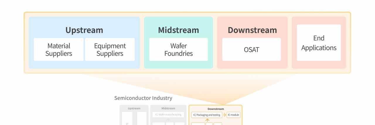
Related Articles:Taiwan Industry 101: Introduction to CoWoS Technology
What is WMCM?
Wafer-Level Multi-Chip Module (WMCM) is an advanced packaging technology developed by TSMC, regarded as an upgraded architecture of InFO-PoP (Integrated Fan-Out Package-on-Package). Unlike traditional single-chip packaging—where wafers are first diced into individual dies and then packaged and soldered onto printed circuit boards—the core concept of WMCM is to complete packaging at the wafer stage, effectively combining wafer-level packaging with heterogeneous multi-die integration.
Core WMCM Technology
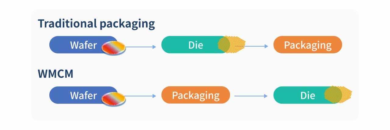
WMCM belongs to the InFO (Integrated Fan-Out) architecture and is structurally similar to the CoWoS-R (Chip-on-Wafer-on-Substrate with RDL) process. Its key feature is the lateral integration of multiple dies—such as AP processors, LPDDR memory, and passive components—into a single package at the wafer stage, which is then diced into individual chips. However, unlike CoWoS, WMCM eliminates the need for substrates or silicon interposers. Instead, chips are embedded directly into molded resin and interconnected via Redistribution Layers (RDL), enabling horizontal signal transmission at the wafer level.
Unlike traditional packaging where I/O is limited beneath the die, the core of Fan-Out architecture is extending signals outward through RDL. This not only increases the number of available I/O connections but also provides more flexibility for vertical stacking or lateral integration of APs and memory. As a result, Fan-Out technology shortens signal paths, reducing power consumption and latency.
Additionally, unlike InFO-PoP, which stacks memory directly on top of logic chips, WMCM adopts a 2.5D integration approach. It places logic chips and DRAM side-by-side in a planar layout instead of vertical stacking. WMCM also features a dual-layer structure: the upper layer contains AP and memory, while the lower layer integrates multiple capacitors. These capacitors, positioned directly beneath the AP and memory, help reduce noise and stabilize power delivery. Integrating capacitors within the same package further shortens interconnect paths, improves signal efficiency, and reduces overall size.
Overall, WMCM increases the number of integrated chips while simplifying the process by eliminating substrates and relying on RDL. This results in improvements in package size, thickness, thermal performance, and signal loss. It can effectively enhance battery life in mobile devices, and by removing substrate requirements, it also offers a lower cost structure compared to other advanced packaging technologies. These advantages make WMCM essential for space-constrained products such as smartphones and communication chips.
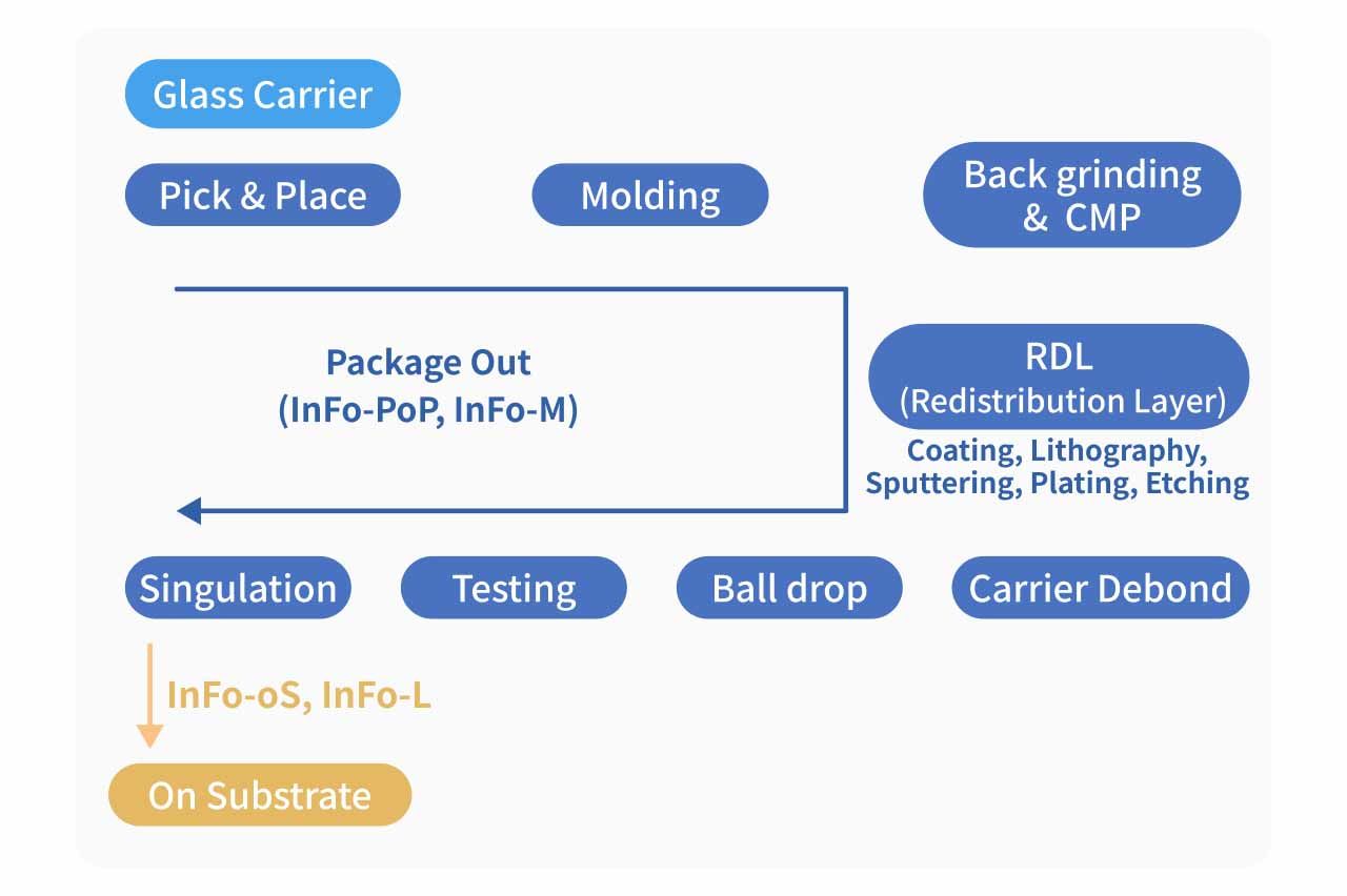
InFO Process Flow
The InFO process consists of nine major steps, from glass carrier handling to wafer singulation. Among them, molding and RDL technologies are the most critical stages.
Detailed Process Overview
1. Glass Carrier
Used as temporary mechanical support, the glass carrier provides structural stability for thin wafers required in heterogeneous integration, preventing breakage or defects during processing and maintaining yield stability.
2. Pick and Place
Known-good dies from front-end processes are individually selected and precisely placed on designated positions on the glass carrier according to the package layout. Since die placement directly determines RDL routing, I/O configuration, power delivery, and thermal design—and cannot be corrected after molding—this step is critical for structural accuracy and yield.
3. Molding
Molding involves evenly applying molding material over the dies and curing it under controlled temperature and pressure. This allows resin to fill gaps between chips, reducing voids and displacement while ensuring uniform wafer thickness. Embedding all dies within molded resin locks them into a single mechanical structure, providing rigidity and stability for subsequent high-stress processes such as grinding, CMP, and multi-layer RDL fabrication.
Traditionally, underfill was applied first, followed by external molding. However, shrinking die spacing and increasing process complexity have created challenges. In the supply chain, Eternal Materials (1717.TW) has introduced MUF (Molded Underfill), integrating underfill and molding into a single step, reducing material usage, shortening process time, and improving yield.
4. Back Grinding / CMP
Back grinding removes excess molding material and reduces die thickness from the backside to achieve target wafer height and uniformity. This is followed by CMP, which uses chemical and mechanical polishing to repair damage and reduce stress, lowering risks of warpage and cracking.
5. RDL (Redistribution Layer) Process
- Coating: Apply dielectric materials such as PI or PBO for insulation and stress buffering.
- Lithography: Define metal routing and vias using photoresist exposure and development.
- Sputtering: Deposit a thin metal seed layer (e.g., Ti, Cr) for adhesion and conductivity.
- Plating: Electrochemically deposit metal to form RDL structures.
- Etching: Remove excess metal to create isolated and well-defined routing patterns.
6. Carrier Debonding
The glass carrier is removed after RDL formation using heat or solvents to release the wafer.
7. Ball Drop
Solder balls are precisely placed on pads to establish mechanical and electrical connections to the PCB.
8. Testing
Electrical, functional, thermal, and reliability tests are conducted to ensure performance and filter out defective chips.
9. Singulation
The wafer is diced into individual chips. Advanced methods such as laser or plasma dicing are increasingly used to reduce edge damage.
Advantages of InFO-M Technology

High-Density RDL Significantly Shortens Interconnect Paths, Improving High-Speed Signal Integrity and Lowering Power Consumption
InFO-M uses a high-density RDL routing structure with three layers and 2/2µm line width/line spacing, without requiring an additional package substrate or TSVs, and supports a package size of less than 500 mm². Compared with InFO-PoP, which also includes three RDL layers but with line spacing ranging from 2–10µm, InFO-M further reduces routing pitch. First, the high-density RDL directly redistributes I/O on the chip, significantly shortening both die-to-die and chip-to-external interconnect paths, so signals no longer need to pass through multi-layer substrate routing or TSV vertical connections. Because RDL line width and spacing can be made far smaller than those of a substrate, interconnect impedance, parasitic capacitance, and parasitic inductance are all substantially reduced, which in turn lowers both crosstalk and power consumption in high-speed signals.
Eliminating the Substrate and TSVs Enables High-Density Multi-Chip Integration
In terms of package size and system integration density, removing the substrate and TSVs effectively compresses both the package height and its lateral footprint. For products with a package area below 500 mm², InFO-M can achieve tight integration of multiple chips or chiplets through multi-layer high-density RDL without introducing an interposer, greatly increasing system integration density. This is especially important for mobile devices and high-performance yet size-constrained AI/HPC edge computing chips, because package area and thickness often directly limit end-product design and thermal layout.
Simplifying the Process Flow and Supply Chain with RDL at the Core
From the perspective of cost structure and yield risk, avoiding the use of substrates and TSVs can significantly simplify the overall supply chain and process complexity. High-end ABF substrates are expensive, have long lead times, and carry clear yield risks as I/O counts and layer numbers increase. TSVs, meanwhile, involve high-cost and yield-sensitive processes such as etching, copper filling, and CMP. With RDL at its core, InFO-M avoids these higher-risk steps, making it more competitive in both per-I/O cost and total packaging cost, while also being better suited for large-scale mass production.
A Simplified Package Structure Allows Heat Sources to Align More Directly with the Thermal Path
In thermal management, a simplified package structure helps improve heat conduction paths and stress distribution. In InFO-M packages, heat sources can couple more directly with the upper thermal solution, reducing the thermal resistance introduced by substrates and TSVs. At the same time, having fewer layers of dissimilar materials reduces coefficient of thermal expansion (CTE) mismatch, which has a positive effect on long-term thermal cycling reliability, warpage control, and the risk of microcracks.
High-Density RDL Provides Routing Flexibility, Striking a Balance Between Performance and Cost
Finally, from a scalability perspective, high-density RDL offers greater routing flexibility than traditional substrates, making it easier for system designers to adopt heterogeneous integration without taking on the cost and risk associated with TSV-based architectures as die size increases. For products aiming to capture benefits similar to a chiplet architecture, InFO-M offers a relatively balanced and scalable solution across performance, cost, and manufacturability.
Limitations of InFO-M
Although InFO-M demonstrates significant advantages in electrical performance, package size, cost structure, reliability, and system integration flexibility—through its high-density RDL, substrate-free, and TSV-free architecture—it still faces certain technical limitations and challenges in real-world mass production and application scenarios.
Planar Scaling Bottleneck from Replacing Substrates with RDL
The primary limitation of InFO-M lies in the planar scaling constraints resulting from replacing substrates with RDL. While high-density RDL features extremely fine line width and spacing, the number of RDL layers is limited, and the total I/O capacity is still constrained by thin-film processing and warpage control capabilities. When very high I/O is required, rapidly increasing RDL layers leads to sharply higher process complexity, yield loss, and cost, making it difficult to support complex chip stacking and high-density interconnects.
Thermal Performance Still Inferior to CoWoS
In terms of power density and thermal limits, although InFO-M offers improved heat dissipation compared to InFO-PoP, its thermal performance still falls short of CoWoS. The molded resin used in InFO-M has relatively low thermal conductivity, making it unsuitable for HPC chips that require extremely high power and sustained full-load operation. Since its core structure remains a thin RDL-based design without a silicon interposer or thick substrate to act as a heat spreader, heat flux can become highly concentrated in localized regions as total power increases across one or multiple dies. In other words, InFO-M is better suited for lower-power, performance-density-driven designs rather than high-power applications.
However, these disadvantages are not flaws but a reflection of its clearly defined positioning. InFO-M is not intended to replace other advanced packaging technologies; instead, it targets applications with moderate package size, high I/O density, extreme sensitivity to electrical performance and form factor, and manageable power and system scale. When applications demand ultra-high I/O integration, high bandwidth, extreme power, or highly modular system-level integration, the structural limitations of InFO-M become more apparent—at which point CoWoS or other 2.5D/3D architectures offer stronger advantages.
Comparison: InFO-M (WMCM) vs. Other Packaging Technologies
| Technology | InFO-PoP | InFO-oS | InFO-L | InFO-M (WMCM) |
|---|---|---|---|---|
| Structure | RDL + TIV, stacked AP + DRAM | RDL + substrate (with TSV) | InFO-R + local silicon interconnect | High-density RDL, no substrate/TSV |
| RDL | 2/2µm | 2/2µm | 0.4/0.4µm | 2/2µm |
| Strength | Thin package | Larger integration | Highest density (HPC) | Lateral integration, better thermals |
| Applications | Apple A-series | Apple M Pro/Max | Apple M Ultra | Future Apple A-series |
Overall, the InFO family is centered around redistribution layer (RDL) technology, but each branch follows a distinct design approach. Among them, WMCM emphasizes high-density RDL-based lateral integration, enabling multi-chip interconnection without the use of substrates or TSVs. This provides structural advantages in signal transmission efficiency and overall thickness control, while also improving thermal performance and reducing signal loss. As a result, it is regarded as a key direction for next-generation advanced packaging, with primary end applications in Apple’s A-series chips, and is expected to become a major adoption starting from the A20 generation.
In comparison, InFO-PoP focuses on combining RDL with TIV and stacking integration of AP and DRAM, with the primary goal of reducing package height and footprint. InFO-oS integrates RDL with substrates and incorporates TSVs to enhance integration flexibility and support larger package sizes, mainly targeting platforms such as Apple’s M Pro and M Max. Meanwhile, InFO-L combines InFO-R with local silicon interconnects to deliver higher interconnect density, making it suitable for high-performance computing scenarios that require integration of multiple logic chips.
Comparison: WMCM vs. CoWoS Family
| Technology | CoWoS-S | CoWoS-R | CoWoS-L | WMCM |
|---|---|---|---|---|
| Packaging | 2.5D | 2.5D | 2.5D | 2.5D |
| Process | Chip Last | Chip Last | Chip Last | Chip First |
| Interposer | Silicon + TSV | Silicon + RDL | Local silicon + RDL | None (RDL only) |
| Cost | High | Medium | Highest | Lowest |
| Applications | HPC, AI | AI ASIC | Large AI models | Mobile devices |
| Products | NVIDIA Hopper | AWS Trainium | NVIDIA Blackwell | Apple Silicon |
WMCM and the CoWoS family are both classified as 2.5D packaging technologies, but their key differences lie in process flow and interposer architecture. CoWoS-S, CoWoS-R, and CoWoS-L all adopt a Chip Last process and rely on interposers to enable high-density interconnects. Among them, CoWoS-S primarily uses silicon interposers with TSVs; CoWoS-R combines silicon interposers with RDL; and CoWoS-L introduces local silicon interconnect (LSI) alongside RDL. These approaches progressively enhance interconnect capability and system scale, but also drive up costs. Their applications are mainly focused on HPC and AI accelerators, including products such as NVIDIA Hopper and Blackwell GPUs, as well as AWS Trainium and other mid-to-high-end AI ASICs.
In contrast, WMCM adopts a Chip First process, eliminates the need for an interposer, and relies solely on RDL for interconnection, with flip-chip packaging as its primary form. This significantly simplifies both material requirements and process complexity, resulting in the lowest cost structure among the four. As such, WMCM is better suited for mobile devices and consumer electronics that are highly sensitive to size, thickness, and cost, with Apple Silicon being a representative end application.
From InFO to WMCM: Evolution and Impact
Currently, smartphone chips widely adopt InFO technology (primarily InFO-PoP), mainly because it offers ultra-thin packaging advantages and enables direct stacking of memory and processors through the PoP structure to save space. However, as sustained high workloads from AI/NPU/GPU in SoCs become more common, and as I/O counts, memory capacity, and bandwidth continue to increase, existing InFO solutions are beginning to face several challenges. These include thermal bottlenecks caused by stacked structures limiting heat dissipation, difficulty in expanding package size to accommodate more chiplets, and increased thickness and process complexity from vertically stacking DRAM.
As the next-generation solution to InFO, WMCM integrates multiple dies more tightly at the wafer level and features higher-density RDL. This not only shortens interconnect distances but also enables more efficient heterogeneous integration and improved thermal layout. If WMCM achieves stable mass production and scaling, its application scope could expand from smartphones to Apple’s M-series processors in MacBooks and R-series chips used in head-mounted devices. Furthermore, as the industry enters the 2nm era and demands stronger AI integration, flagship chips from Qualcomm and MediaTek are highly likely to upgrade from existing InFO solutions to WMCM to push performance limits.
However, market estimates suggest that WMCM packaging costs around $3,000–$4,000 per unit, significantly higher than InFO’s $1,500–$1,800. This implies that material and equipment investment intensity per unit will also increase accordingly. Before WMCM’s performance advantages are fully validated, its adoption timeline may remain constrained.
| Item | InFO_PoP | WMCM |
|---|---|---|
| Packaging Type | Fan-out wafer-level packaging | Wafer-level multi-chip module |
| Number of Dies | 1 | 2–4 |
| Integration Method | Vertical stacking, PoP (Package on Package) | Horizontal (side-by-side) |
| Process Node | 3nm, 5nm | ~2nm |
| RDL Layers | 1–2 layers for basic I/O redistribution | 2–3 layers supporting multi-die interconnect |
| Target Power | 3–10W | 5–25W |
| Chip Size | Larger | Smaller |
| Package Thickness | Increases with memory stacking | Thicker, but better controlled |
| Thermal Performance | Challenged as stacking increases | Improved |
| Cost | Lower | Higher, but lower than CoWoS |
| Mass Production | Since 2016 | 1H26 |
Beneficiary Taiwanese Companies
C Sun (2467.TW)
Company Overview
C Sun (2467.TW), established in 1966, focuses on developing key process equipment required for advanced packaging and IC substrates, including lamination, bonding, debonding, baking, and wet process technologies for pre-plating treatment. Its products are widely used across industries such as PCB, FPD, semiconductors, and advanced packaging.
C Sun operates manufacturing facilities in Taipei, Taichung, Guangzhou, and Kunshan. Its semiconductor clients include TSMC (2330.TW) and ASE Technology Holding (3711.TW), while in the PCB sector, its customers include Unimicron (3037.TW), Wus Printed Circuit (002463.SZ), and Victory Giant Technology (300476.SZ), all of which are global industry leaders.
Growth Driver 1: TSMC Promotes Localization of Advanced Packaging Equipment, Increasing Exposure to Major Clients
According to TSMC’s ESG report, by 2030 the company aims to reach local procurement ratios of 50% for raw materials, 68% for components, and 38% for backend equipment, as local suppliers can provide more timely support compared to overseas vendors. Currently, Taiwanese vendors account for only about 10% of the backend equipment market, implying 3–4x growth potential.
In addition, in 2020, C Sun formed the G2C+ alliance with Gallant Precision (5443.TWO) and Gallant Micro. Machining (6640.TWO) to promote the localization of advanced packaging equipment in Taiwan. The company is expected to continue benefiting from localized capital expenditure trends, as reflected in the rising share of revenue from Taiwanese customers—primarily driven by capacity expansion plans from TSMC and ASE.
Beyond advanced packaging, strong AI demand is driving increased capital expenditure in the PCB industry. Major manufacturers such as Zhen Ding (4958.TW), Unimicron (3037.TW), Gold Circuit Electronics (2368.TW) , and Victory Giant (300476.SZ) are significantly increasing capex this year and next. Meanwhile, amid de-China trends, companies such as Shengyi Electronics (688183.SZ), Dynamic Holding (3715.TW), Unimicron (3037.TW), and Victory Giant (300476.SZ) are expanding production in Southeast Asia, further boosting demand for PCB equipment.
Growth Driver 2: Entering the WMCM Supply Chain with Photolithography Heating Equipment and Backend Industrial Ovens
In WMCM packaging, C Sun provides photolithography heating equipment used in wafer-level packaging to precisely heat and bake photoresists or dielectric layers, ensuring process stability. Since WMCM requires significantly more RDL layers than InFO packaging, the number of curing cycles also increases accordingly. This leads to higher equipment utilization rates and increased demand for such systems.
In addition, WMCM processes involve a wide range of materials. Differences in coefficients of thermal expansion (CTE) during heating and cooling can easily cause wafer warpage and stress issues. As RDL layers increase, dielectric layers, metal layers, and lithography cycles also rise, intensifying thermal cycling and interlayer stress accumulation. This further amplifies risks such as warpage, misalignment, and yield loss. C Sun’s photolithography heating equipment provides highly precise temperature control and ramping profiles, ensuring wafer flatness during multi-layer processing.
WMCM equipment pricing is comparable to CoWoS, and the market expects related equipment to contribute a mid-single-digit percentage to C Sun’s 2026 revenue.
In backend packaging, WMCM adopts MUF (Molded Underfill), which integrates underfill and molding into a single process, simplifying steps and improving thermal performance. After material injection, long-duration post-curing in precision industrial ovens is required to achieve the desired mechanical strength and thermal stability. C Sun’s industrial ovens position the company to enter backend packaging processes, creating additional upside potential.
Eternal Materials (1717.TW)
Company Overview
Eternal Materials (1717.TW), founded in 1964, is a leading global supplier of synthetic resins and electronic chemical materials. Its core business spans three major segments: synthetic resins, electronic materials, and specialty chemicals, with applications across PCB, automotive, construction coatings, and consumer electronics.
The company operates production bases worldwide, including Taiwan, China, the U.S., Japan, and Thailand. Leveraging strong technical expertise, Eternal Materials has become a supplier to Apple and has secured orders for advanced packaging materials from TSMC, serving major global players in electronics, communications, and manufacturing.
Underfill as a Critical Process in Chip Packaging
Underfill is a key process in flip-chip packaging that enhances reliability. Due to differences in CTE between the chip and substrate, thermal cycling can generate stress at solder joints, increasing the risk of failure. Underfill fills the gaps between solder bumps, redistributing stress, improving mechanical strength, and enhancing thermal performance as well as moisture and corrosion resistance.
Mainstream underfill approaches include Capillary Underfill (CUF) and Molded Underfill (MUF).
CUF: High Reliability but Slower Throughput
CUF is a post-fill process where epoxy is dispensed along the chip edge after reflow or bonding, and capillary action draws the material into the gap. It offers high reliability and relatively uniform filling with low void risk, making it common in high-end CPUs/GPUs and applications that prioritize reliability, such as smartphone APs and HPC chips.
However, CUF requires sequential dispensing, flow, and curing, resulting in slower throughput. In addition, insufficient flux cleaning can affect fill quality.
MUF: Better Aligned with WMCM Requirements
MUF is an integrated packaging process in which epoxy molding compound (EMC) is injected via transfer molding after die placement, simultaneously achieving underfill and encapsulation. Compared with CUF, MUF significantly shortens cycle time, reduces equipment costs, and lowers process risks associated with repeated high-temperature steps.
As processes move to 2nm and bump pitch continues to shrink, CUF becomes less effective at filling tiny gaps due to reliance on capillary action, increasing void risk. MUF, by contrast, uses pressure-driven molding to improve fill quality and yield, making it more suitable for WMCM’s high-density, thin-profile, and high-volume requirements.
From a materials perspective, using different materials for CUF and outer molding can create CTE mismatch and severe wafer warpage in large-area packages. MUF uses a unified material system, resulting in more even stress distribution—particularly beneficial for 12-inch wafer-level packaging like WMCM.
Eternal Materials Gains Share with Low-Warpage, High-Adhesion EMC
WMCM’s adoption of MUF introduces challenges in fill uniformity, material properties, and stress control. EMC must offer both low viscosity and high flowability, while filler particle sizes must shrink to enter fine gaps. In addition, mismatched CTE between EMC, chips, and substrates can lead to thermal stress and warpage.
Eternal Materials has leveraged its low-warpage materials and strong adhesion to silicon and copper interfaces to gain market share from Japanese competitors such as Namics and Nagase. It has secured advanced packaging material orders from TSMC, supplying MUF materials for Apple’s latest iPhones and Mac processors. As of 3Q25, MUF accounted for only 0.3–0.4% of total revenue, but wafer-level liquid packaging materials are expected to ramp up between 2Q26 and 3Q26, potentially reaching around 5% of revenue by 2026–2027.
