

The Open Compute Project (OCP) is an open-source hardware initiative launched in 2011 by companies including Meta, Intel, Rackspace, and Goldman Sachs. It aims to open up traditionally closed specifications for server and data center hardware. By publishing open specifications for servers, storage equipment, rack designs, and data center infrastructure, OCP encourages technology companies and supply chain partners worldwide to develop products collaboratively, advance hardware standardization, and improve system interoperability. The OCP Global Summit is the organization’s annual flagship event, bringing together hyperscalers, major chipmakers, and hardware manufacturers to showcase and discuss key technologies in AI servers, data center power delivery, liquid cooling, and high-speed networking. The 2026 summit’s theme was “Scaling Innovation for the AI Era.” As AI moves toward agentic AI, models require not only greater compute power but also more efficient inference, greater memory capacity and bandwidth, and faster data transfer within clusters. This year’s technical focus on optical communications, orthogonal backplane switches, 3.5D advanced packaging, and memory reflects a broader shift in AI infrastructure: competition is moving beyond the performance of individual chips toward system-wide upgrades in compute, data transmission, memory, power, and cooling.
Optical Interconnects Meet Growing AI Compute Demand: NPO and Open Architectures Draw Attention
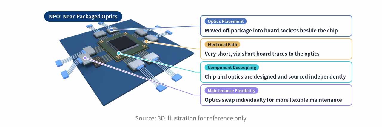
Optical communications were a major theme at the 2026 OCP Global Summit, reflecting how bottlenecks are increasingly shifting toward data transmission and interconnect efficiency as AI models grow, accelerator counts rise, and data center compute density increases. On the second day of the summit, IPEC hosted an optical interconnect workshop attended by companies including Source Photonics, LightCounting, Alibaba, Meta, Oracle, Microsoft, Ciena, Lumentum, NVIDIA, and Huawei. The session focused on the development and commercialization prospects of near-packaged optics (NPO), which places optical components closer to compute or switching chips to shorten electrical transmission paths, increase bandwidth density, and reduce power consumption. Compared with co-packaged optics (CPO), NPO offers advantages in component separation and maintenance flexibility. Open architectures such as Open CPX also drew interest, with the goal of reducing equipment integration complexity through standardized cross-vendor interfaces.
The third day’s forum focused on photonics, with companies including NVIDIA, Meta, Microsoft, Oracle, Broadcom, Celestica, Arista, Ciena, Amphenol, Lumentum, and Huawei sharing their technology roadmaps. The industry generally expects CPO and NPO to develop in parallel for different applications. Performance, power consumption, cost, deployment speed, and reliability will be key factors in evaluating adoption. The forum noted that approximately 83% to 85% of CPO failures are associated with external laser sources (ELS), while around 11% to 17% involve optical fibers or connectors—highlighting the importance of reliability and maintenance to commercial deployment. At the system level, scale-up systems with more than 576 accelerators are expected to move toward all-optical pods, while systems with 72 to 576 accelerators are expected to use optical and copper interconnects in parallel.
Overall, optical communications have become a key technology for increasing compute density and energy efficiency in AI data centers. Over the longer term, CPO may benefit from demand for greater integration and bandwidth. In the near term, however, NPO’s maintenance flexibility and the technical challenges associated with CPO leave room for further development. The two approaches are likely to evolve in complementary ways, each serving different applications and system requirements.
Cisco Unveils the World’s First USFP Optical Communications Module
NVIDIA and Cisco introduced the next-generation Ultra-Dense Small Form Factor Pluggable (USFP), which they co-developed, at the 2026 OCP Global Summit. Targeting the 400 Gb/s-per-lane electrical transmission generation, the companies plan to use an open industry specification to encourage participation from multiple suppliers. Existing pluggable modules such as OSFP connect to host-side connectors through contacts arranged along the edge of a circuit board. As data rates rise to 400G per lane, the high-frequency performance of contacts, connectors, and traces becomes a design challenge. USFP instead uses a two-dimensional array connector and a two-stage insertion mechanism: the module is first positioned, then its high-speed contacts engage. This design aims to improve signal integrity and reduce contact wear. According to the companies, USFP is expected to deliver four times the bandwidth density and approximately 1.3 times the power efficiency of pluggable optical modules operating at 200 Gb/s per lane. The module does not require a dedicated built-in liquid-cooling loop, preserving the serviceability and deployment convenience of a pluggable design.
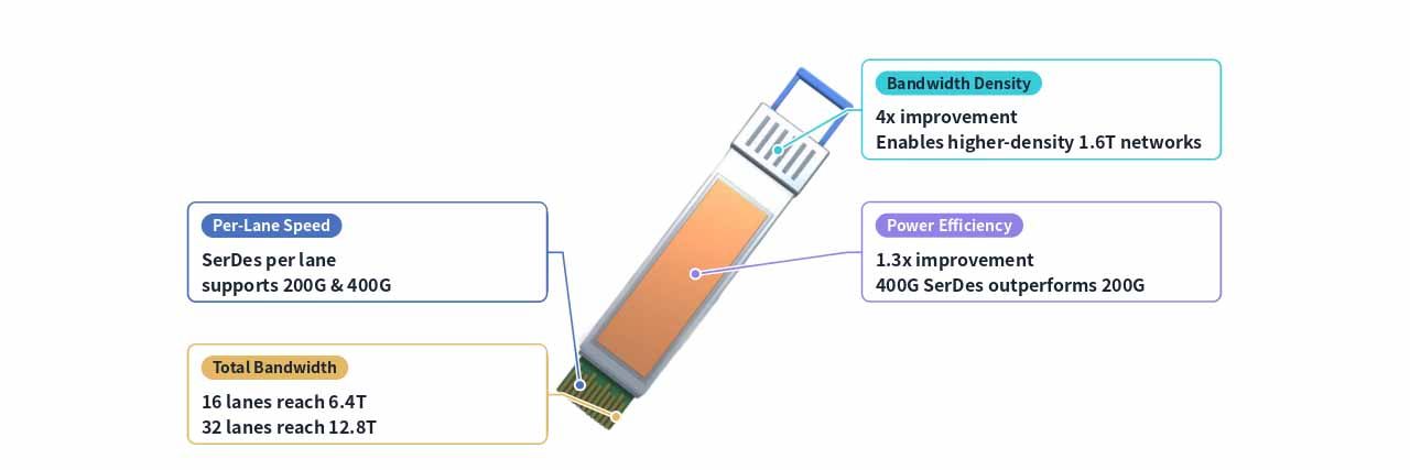
Current solutions include OSFP and XPO. OSFP benefits from a mature industry ecosystem, a complete supply chain, and maintenance and deployment processes that customers already know. XPO uses more lanes to increase total bandwidth per module and incorporates cooling features such as liquid cooling into the module design. It targets very high front-panel bandwidth density, but adds mechanical, thermal, and maintenance complexity.
USFP takes a different approach: it increases the data rate per lane and uses 400G per lane to deliver more bandwidth in a similar module footprint, while retaining a pluggable design and avoiding a dedicated liquid-cooling loop within the module. In other words, XPO aims to increase density by adding lanes and integrating liquid cooling, while USFP seeks to use a faster electrical interface to balance density, power consumption, and ease of maintenance within a pluggable architecture.
For NVIDIA, USFP could help integrate switches and SuperNICs, increase bandwidth density in AI networks, reduce the number of network tiers and their associated power demands, and broaden hardware sourcing and customer adoption options through an open specification. For Cisco, USFP is a strategic move to participate in next-generation high-speed Ethernet and optical communications standards. Through its collaboration with NVIDIA, Cisco can combine its Silicon One switch chips, networking equipment, and optical technologies to strengthen its overall solutions. A multi-supplier ecosystem could also broaden industry participation and increase Cisco’s influence in the next-generation AI networking supply chain.
Overall, USFP’s launch reflects a shift in AI networking competition beyond simply increasing optical module data rates. Electrical interfaces, connectors, cooling, and overall system architecture are increasingly being designed together. Compared with existing form factors such as OSFP, USFP aims to use 400G per lane to increase bandwidth density while preserving the serviceability and deployment advantages of pluggable modules. Compared with XPO, which uses more lanes and in-module liquid cooling, USFP pursues density and system simplification through faster per-lane signaling.
HGGenuine Showcases 3.2T, 6.4T NPO, and 12.8T XPO Solutions at Its First OCP Summit
HGGenuine, an optical communications equipment subsidiary of China’s HGTECH, made its first appearance at the 2026 OCP Global Summit, showcasing three solutions for next-generation high-speed optical interconnects in AI data centers: 3.2T optical modules, 6.4T near-packaged optics (NPO), and 12.8T ultra-high-density pluggable optics (XPO).
The 3.2T optical module uses 400G per wavelength and a DSP chip manufactured on a 3 nm or 2 nm process. Its per-wavelength transmission rate can reach up to 450 Gbps, and it is compatible with existing data center architectures, helping customers upgrade network bandwidth. The 6.4T NPO solution uses a DSP-free linear-drive architecture and supports single-mode fiber transmission over distances of up to 500 meters. According to the company, compared with a conventional 800G OSFP pluggable optical module, it delivers 11.4 times the bandwidth density per unit area and reduces energy consumption per bit by 50%. This could improve data transmission efficiency in AI compute clusters while lowering the power burden of high-speed interconnects.
The 12.8T XPO uses 64 lanes at 200G per wavelength, with module power consumption as low as 130W. It can increase switch rack density by four times, addressing AI data centers’ demand for greater bandwidth and density, as well as improved energy efficiency. HGGenuine is also a founding member of the XPO MSA standards consortium. By participating in the development of next-generation optical interconnect specifications, the company is strengthening its position in high-speed optical communications and industry standards.
In addition to high-speed optical modules, HGGenuine is expanding upstream into optical chips and light-source technologies. Its work includes in-house silicon photonics chips and external laser sources using quantum-dot optical frequency combs (ELSFP). The company has established three optoelectronics manufacturing platforms—indium phosphide (InP), gallium arsenide (GaAs), and silicon photonics (SiP)—and is also developing thin-film lithium niobate technology. These efforts are intended to expand its in-house capabilities in high-speed optical chips and light sources and strengthen control over key component supply.
In the first half of 2026, the company began volume shipments of 800G and 1.6T high-speed optical modules worldwide and continued to expand its North American cloud customer base. This suggests that its existing high-speed optical communications products have established a foundation for production and delivery. As AI models and compute clusters continue to scale, HGGenuine is looking to capture opportunities from the next wave of AI infrastructure upgrades.
NVIDIA’s Orthogonal Backplane Upgrade: PTFE High-Speed Materials and Supply Chain Positioning
Upgrades to NVIDIA’s next-generation AI rack architecture are increasing the importance of high-speed interconnects and PCB materials. As Rubin Ultra and the subsequent Feynman generation move toward greater GPU integration and bandwidth, NVIDIA’s planned Kyber rack uses vertically inserted compute trays connected by an orthogonal backplane. This design aims to reduce the use of conventional copper cables, simplify cabling, save space, and improve signal integrity and cooling.
Because backplanes and switch boards must maintain signal quality at extremely high data rates, the copper-clad laminate (CCL) materials used in PCBs are also drawing market attention. The main materials under discussion are glass-fiber-free CCLs based on either hydrocarbon resin (HC) or polytetrafluoroethylene (PTFE). HC offers potential in materials and process development, but still needs to meet electrical requirements such as dielectric loss in extremely high-frequency applications. PTFE has low dielectric loss, low moisture absorption, and good high-frequency stability, which can help reduce signal attenuation during high-speed transmission. Its glass-fiber-free structure can also reduce local variations in dielectric properties and signal propagation time caused by woven glass fabric. PTFE nevertheless presents challenges involving processing difficulty, panel dimensional stability, copper bonding, manufacturing yield, and cost.
At the 2026 OCP Global Summit, a collaboration display featuring an NVIDIA-related NVLink PTFE switch board drew market attention. Related supply chain companies include Taiwan’s Taiflex Scientific (8039.TW) and Flexium Interconnect (6269.TW); China’s Victory Giant Technology, Shennan Circuits, Kinwong Electronic, and Shengyi Technology; and U.S.-based TTM Technologies.
Among Taiwan’s suppliers, Taiflex is focused on PTFE copper-clad laminate materials. By combining PTFE with fillers and glass-fiber-free designs, the company is seeking to meet demand for next-generation high-speed switch boards. If its products pass customer qualification and enter mass production, it could expand its presence in the high-end, high-speed materials market. Flexium focuses on flexible printed circuit boards and high-speed interconnect technologies. It is also developing high-end materials such as modified polyimide (PI), liquid crystal polymer (LCP), and PTFE. Combining its material development with circuit design capabilities could create opportunities to participate in high-end interconnect solutions for next-generation AI infrastructure.
Overall, PTFE still faces technical challenges involving processes, yield, and cost. However, its appearance in a collaborative showcase for an NVIDIA-related NVLink switch board at OCP signals that it is becoming an important material direction for next-generation high-speed interconnects. As AI racks evolve toward greater bandwidth and integration, PTFE could become a long-term material option for high-end switch boards and backplanes. For Taiwan’s Taiflex and Flexium, key factors to watch include the validation and mass-production progress of PTFE CCL, as well as whether high-end materials and interconnect solutions are adopted for next-generation platforms on schedule.
Emerging AI Infrastructure Trends: Advanced Packaging, Memory, and Rack Architecture
3.5D Advanced Packaging
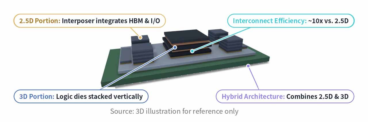
As 2.5D packaging approaches its physical limits, MediaTek expressed optimism about the potential of 3.5D packaging at this year’s OCP Global Summit, describing it as a technology that could extend the performance of high-end chips. 3.5D is a hybrid architecture that combines 2.5D and 3D integration. It vertically stacks logic chips and uses an interposer to integrate components such as HBM and I/O, increasing chip integration and interconnect efficiency. MediaTek said its custom ASIC designs can support chip sizes approaching 10 times the reticle limit, and that 3.5D integration can improve chip-to-chip interconnect energy efficiency by approximately 10 times compared with conventional 2.5D packaging. The company expects related applications to continue growing over the next three to five years. Design-technology co-optimization (DTCO) for custom HBM and proprietary chip-to-chip interconnects will also be an important area of development. As AI chip architectures become more complex and demand for data interconnects rises, 3.5D advanced packaging could see further structural growth opportunities.
SK hynix Presents Its Latest Memory Architecture
To address memory capacity and key-value cache (KV-cache) bottlenecks in large-scale AI inference, SK hynix Senior Vice President Kim Ho-sik introduced MARS (Memory-Centric AI Rack-Scale System), a rack-scale memory system, at the OCP Global Summit. By decoupling compute and memory resources, MARS creates a memory pool that can be shared across multiple servers. This can improve resource allocation efficiency, reduce GPU overprovisioning, and lower total cost of ownership.
SK hynix is also developing high-bandwidth flash (HBF), which uses stacked NAND to offer a capacity and bandwidth tier between HBM and SSDs. It is designed for large inference data such as model weights and long-context KV caches. At the same event, the company introduced its second-generation 256GB CXL 3.2 memory product. Through memory pooling and dynamic allocation, the product increases system scalability, more than doubles bandwidth compared with its predecessor, and improves energy efficiency by approximately 30%.
Overall, SK hynix is not positioning HBF as a replacement for HBM. Instead, it is using a tiered combination of HBM, HBF, and CXL to meet distinct needs for high-speed compute, high-capacity storage, and flexible scaling. As AI inference and multi-turn conversations increase memory demand, interconnect technologies between chips and servers will also be critical to improving memory sharing and access efficiency, driving further evolution in AI memory architecture.
Agentic AI Raises the Importance of CPUs, Bringing CPU Racks Into Focus
As AI evolves from generative AI toward agentic AI, data center compute demand is expanding beyond GPU inference to include the general-purpose computing and task coordination handled by CPUs. AI agents call models for inference, but also frequently call APIs, query databases, run code, and interact with enterprise systems. As the number of agents and the degree of parallel task execution increase, demand for CPU cores, memory, and I/O resources will also rise.
At the summit, AMD CEO Lisa Su said agentic AI is driving rapid growth in the data center CPU market. AMD has revised its market forecast upward three times in the past nine months and expects a compound annual growth rate of approximately 50% over the next four to five years, with the market exceeding $200 billion by 2030.
To address this trend, AMD, Intel, and NVIDIA each introduced CPU rack architectures at the OCP Global Summit. AMD’s Helion offers flexible configurations, including CPU-only racks with up to 32,768 CPU cores and fully integrated systems combining EPYC CPUs, Instinct GPUs, and a Token Router. Intel showcased high-density Xeon CPU racks, with some configurations offering more than 46,000 CPU cores. They use open standards such as OCP Open Rack v3 and are designed to increase the number of AI agents a single rack can support under specific latency requirements. NVIDIA has incorporated its Vera CPU Rack into its AI Factory architecture. Built on the open, modular MGX platform, it integrates compute, networking, power, and cooling. The rack is designed to handle tool calls, task coordination, and sandbox execution for AI agents, working alongside Vera Rubin GPU systems.
Overall, agentic AI is moving CPUs beyond their traditional supporting role. Dedicated rack architectures that integrate CPUs and related resources are becoming important infrastructure for large-scale agent execution.
AMD Helios and Helion Racks
AMD Chair and CEO Lisa Su also delivered a keynote at the OCP Global Summit titled “Building the Next Era of AI Infrastructure,” focusing on the development of rack-scale AI systems and the industry significance of open architectures.
AMD-led Helios racks use the OCP wide rack standard. Co-designed with Meta, they can integrate 72 GPUs to work together and began volume shipments in September 2026. AMD also introduced Helion racks for agentic AI, integrating CPUs, GPUs, liquid cooling, and a Token Router. They are expected to become available in November, with related specifications to be shared with the OCP community. Alongside its sixth-generation EPYC Verano processors, which are expected to enter volume production in the first half of 2027, AMD is building out its AI infrastructure portfolio from chips to racks.
For the market, Helios matters not only as a high-performance AI system alternative to NVIDIA, but also because its open specifications and standardized design could reduce customers’ dependence on a single vendor’s hardware and software ecosystem, while giving them more flexibility in system integration and supply chain selection. Notably, eight of Helion’s 13 partners are Taiwanese companies: Hon Hai (2317.TW), QCT (a subsidiary of Quanta Computer), Wiwynn (6669.TW) Corporation (a subsidiary of Wistron), MiTAC (3706.TW), Inventec (2356.TW), ASUSTEK (2357.TW), ASRock (3515.TW), and GIGA-BYTE (2376.TW). This could create new growth opportunities for Taiwan’s suppliers.
Summary: AI Infrastructure Competition Is Shifting From Chip Performance to High-Speed Transmission and System Integration
Overall, the 2026 OCP Global Summit showed that competition in AI infrastructure is expanding beyond the compute performance of individual chips to include high-speed transmission. As GPU counts and model sizes grow and agentic AI workloads increase, data exchange between compute nodes is rising rapidly. Transmission bandwidth, latency, and power consumption are becoming key factors in overall compute efficiency.
From optical communications technologies such as USFP, NPO, and CPO to orthogonal backplanes, 3.5D advanced packaging, and next-generation memory interconnect architectures, the industry is working to overcome the limits of conventional electrical interfaces and interconnect designs. The goals are to increase bandwidth density, reduce transmission power consumption, and prevent data transfer from becoming a bottleneck to AI compute expansion. As AI clusters continue to grow, high-speed transmission will be more than the foundation for connecting compute chips; it will also be a key factor in determining the performance and scalability of large-scale AI systems.
Rack demonstrations at the 2026 OCP Global Summit also highlighted the shift toward integrated AI infrastructure. Power companies such as Lite-On Technology (2301.TW), Delta Electronics (2308.TW), and AcBel Polytech (6282.TW) showcased high-voltage DC power solutions, including 800VDC and ±400V. Wistron (3231.TW), Wiwynn (6669.TW), and ASUSTEK (2357.TW) presented rack solutions built on NVIDIA Vera Rubin or AMD Helios platforms, integrating compute, power delivery, and liquid cooling.
Overall, competition in future AI infrastructure will extend beyond chip performance to the coordinated design and integration of power delivery, cooling, data transmission, and compute.
