TSMC, the world’s leading pure-play foundry, maintains a significant technological edge, particularly in advanced process technologies. Beyond using its financial results to gauge the direction of the semiconductor industry, the market also closely watches how its technology roadmap shapes the global supply chain. As a result, this year’s TSMC Technology Symposium has become a key indicator for tracking future developments in advanced process technologies, advanced packaging, and AI.
Semiconductor Market Outlook
TSMC believes the semiconductor market is growing faster than previously expected. While earlier forecasts projected the global semiconductor market would reach $1 trillion by 2030, the company now expects the market to surpass $1 trillion as early as this year and expand further to $1.5 trillion by 2030. The primary growth drivers are the rapid expansion of AI and high-performance computing (HPC) demand. TSMC estimates that by 2030, HPC and AI will account for 55% of the semiconductor market, smartphones around 20%, and automotive and Internet of Things (IoT) applications approximately 10% each. This highlights a clear industry shift from traditional consumer electronics toward AI computing, inference, and data center infrastructure.
In addition, TSMC emphasized that AI is evolving beyond generative AI and agentic AI toward physical AI. As the focus shifts from training to large-scale inference, growing demand for token generation is expected to drive greater investment in AI systems, creating a positive cycle of more AI applications, more tokens, greater computing demand, and higher semiconductor consumption.
Advanced Process Technology Roadmap Update
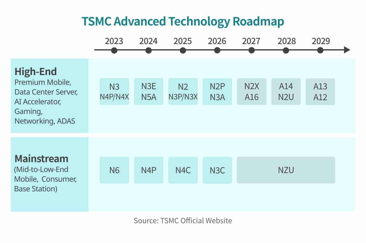
N2 Family: Rapid Ramp-Up from 2025 to 2028
| Process Technology | Mass Production Timeline | Key Highlights |
|---|---|---|
| N2 | Entered production in 4Q25 | First-generation nanosheet technology |
| N2P | Expected in 4Q26 | Enhanced version of N2 |
| A16 | Production expected to begin in 4Q26 | Equipped with Super Power Rail |
| N2X | Expected in 2027 | High-performance variant |
| N2U | Expected in 2028 | Extension of N2P balancing HPC and smartphone applications |
TSMC stated that N2 has officially entered mass production, with more than 25 completed tape-outs and over 70 customer designs currently in development. First-year wafer output is expected to be 45% higher than N3. Furthermore, N2 and A16 capacity will enter a rapid expansion phase between 2026 and 2028, with a projected compound annual growth rate (CAGR) of 70%. Yield learning curves are also outperforming those of N3.
The final member of the family, N2U, delivers a 3–4% performance improvement, 8–10% lower power consumption, and up to 3% higher logic density compared with N2P. This demonstrates that the N2 family, like the previous N5 and N3 generations, is being developed as a comprehensive platform rather than a single-node offering.
A14: Mass Production in 2028 with Second-Generation Nanosheet Transistors
A14 is TSMC’s next major advanced process technology following N2, featuring second-generation nanosheet transistors and NanoFlex™ Pro technology. Compared with N2, A14 can deliver up to 15% higher performance at the same power level or reduce power consumption by up to 30% at the same performance level. It also offers substantial density improvements, with logic density reaching approximately 1.23 times that of N2 and overall chip density about 1.2 times higher.
More importantly, TSMC indicated that A14 has already attracted strong adoption interest from major customers, positioning it as a key process platform for AI, HPC, and premium smartphone chips after 2028.
A13: Mass Production in 2029 as a Direct Shrink of A14
A13 is a shrunk version of A14 with fully backward-compatible design rules, allowing customers to migrate A14 designs to A13 more efficiently. Compared with A14, A13 reduces die area by approximately 6% while further improving power efficiency and performance. Production is expected to begin in 2029.
This indicates that TSMC is not launching A14 as a standalone node but is simultaneously planning A13 as an extension platform, enabling customers to leverage existing designs, lower migration costs, and continue benefiting from power, performance, and area (PPA) improvements.
CFET: Innovation Beyond the Nanosheet Era
TSMC noted that transistor architectures have evolved from planar structures to FinFETs and then to nanosheet designs. Beyond nanosheets, one of the leading candidates for the next-generation technology is CFET (Complementary Field-Effect Transistor), which vertically stacks nFETs and pFETs to further reduce chip area.
TSMC has already demonstrated two key achievements:
- The world’s smallest functional 6T SRAM cell, with a layout area approximately 30% smaller than conventional nanosheet designs.
- A CFET ring oscillator consisting of roughly 1,000 transistors.
Overall, TSMC has begun showcasing its technology portfolio for the post-nanosheet era, although these innovations remain in the research and development stage and have not yet been assigned a specific production timeline.
Comprehensive Expansion of Advanced Packaging
CoWoS: Larger Packaging Sizes with Strong Yield Performance
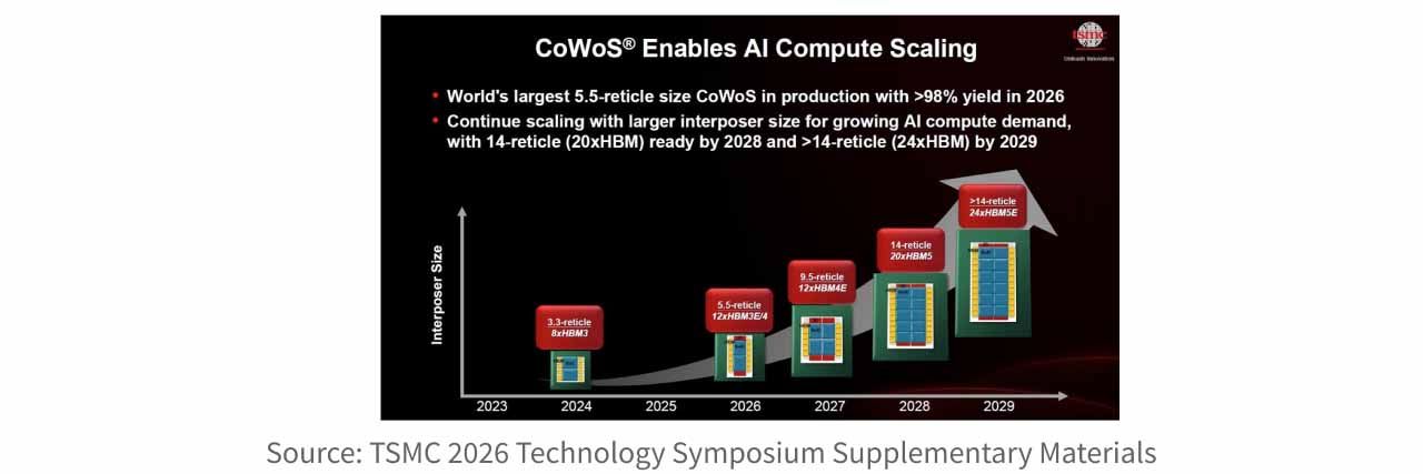
CoWoS is a critical enabling technology for AI training and inference, and most mainstream AI chips currently use CoWoS packaging. TSMC continues to advance the technology and has announced production of the world’s largest 5.5-reticle-size CoWoS package this year, achieving yields above 98%.
Looking ahead, CoWoS will continue to evolve on an annual update cycle. TSMC plans to introduce a 14-reticle-size package in 2028 capable of integrating 20 HBM stacks, followed by a package exceeding 14 reticle sizes in 2029 that can integrate 24 HBM stacks. This underscores TSMC’s leadership in advanced packaging scale, integration capability, and manufacturing yield.
SoW: Wafer-Level System Integration for Larger-Scale AI Computing
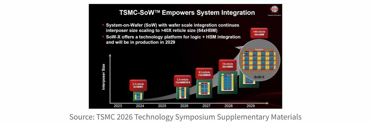
To meet the rapidly growing computational demands of AI training and inference, TSMC announced that it will introduce SoW-X (System-on-Wafer) technology in 2029. The earlier SoW-P platform, designed for logic die integration, entered production in 2024. SoW-X will feature an unprecedented 40-reticle-size format capable of integrating up to 64 HBM stacks and 16 compute chips, positioning it as a larger-scale AI system integration platform beyond CoWoS.
Its primary objective is to overcome single-package size limitations and support significantly higher compute density and larger-scale AI workloads.
SoIC: Significant Gains in 3D Interconnect Density and Power Efficiency
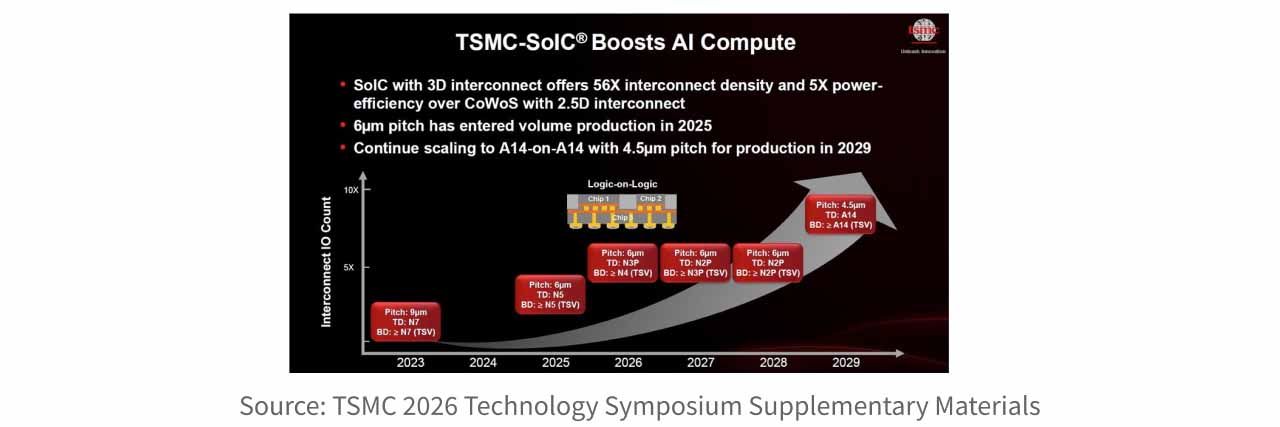
While CoWoS primarily provides 2.5D horizontal interconnects, SoIC introduces 3D vertical stacking capabilities. Together, the two technologies form the foundation of TSMC’s advanced packaging platform. According to TSMC, SoIC offers 56 times higher interconnect density and five times greater power efficiency than CoWoS.
The company has already mass-produced 9-micron-pitch technology and plans to launch 6-micron N2-to-N2 stacking in 2028, followed by a 4.5-micron-pitch A14-generation stacking solution in 2029 to address customer demand for higher AI performance and integration density.
On the capacity front, TSMC is aggressively expanding both CoWoS and SoIC production. From 2022 to 2027, capacity is expected to grow at a CAGR of more than 80%, supporting strong AI-driven demand. Going forward, AI chip architectures will increasingly rely on CoWoS for horizontal integration and SoIC for vertical integration, creating a comprehensive platform that combines both 2.5D and 3D packaging technologies.
COUPE: Optical Interconnects Enter TSMC’s Technology Roadmap
One of the biggest highlights of this year’s Technology Symposium was COUPE (Compact Universal Photonic Engine), marking the formal inclusion of optical interconnect technology in TSMC’s roadmap. The company stated that as data bandwidth requirements and power efficiency become increasingly important, COUPE could emerge as a key technology platform for future systems.
COUPE will integrate co-packaged optics (CPO) solutions. Compared with traditional copper interconnects, a CPO system equipped with COUPE on the substrate can deliver four times greater power efficiency and reduce latency by 90%. When COUPE is integrated directly into the interposer, power efficiency can improve by up to ten times while latency is reduced by 95%.
In addition, the world’s first 200Gbps micro-ring modulator (MRM) using COUPE technology is scheduled for mass production in 2026. TSMC also plans to develop 400Gbps modulators, multi-wavelength technologies, and multi-row fiber arrays, with a target of achieving bandwidth density of 4Tbps/mm by 2030.
This indicates that CPO is no longer solely a topic for networking equipment and switch vendors. Instead, it has been formally incorporated into TSMC’s advanced packaging and system integration roadmap and could become a critical technology for scaling future AI servers.
Conclusion
Overall, this year’s TSMC Technology Symposium once again reinforced the company’s leadership in advanced process technologies, advanced packaging, and system-level integration, while providing a key reference point for the semiconductor industry’s long-term growth trajectory. TSMC raised its outlook for the global semiconductor market to $1.5 trillion by 2030 and clearly identified AI and HPC as the primary growth drivers, highlighting the industry’s ongoing transition from traditional consumer electronics toward AI computing, inference, and data center infrastructure.
At the same time, TSMC continues to build a comprehensive advanced process technology platform. On the packaging side, its roadmap signals that AI chip development has entered a new phase in which front-end process technology, back-end packaging, and system architecture jointly drive performance improvements.
More importantly, the inclusion of COUPE in the technology roadmap demonstrates that optical interconnects and CPO are expanding beyond networking switches into advanced packaging and AI system integration platforms. These technologies could become critical solutions for overcoming future bandwidth, power consumption, and latency bottlenecks.
Taken together, TSMC’s technology roadmap not only validates the continued expansion of AI computing demand but also has significant implications for long-term investment trends across the broader supply chain, including advanced semiconductor equipment, CoWoS and SoIC packaging, HBM memory, CPO technologies, thermal management, and power infrastructure.
