As the Moore era continues to advance, Moore’s Law is steadily approaching its physical limits. Chip dimensions keep shrinking, and process nodes have moved from the nanometer scale toward the angstrom era. With transistor density still rising and the number of stacked layers continuing to increase, traditional 2D chip architectures are gradually nearing their ceiling, and manufacturing is accelerating toward 3D integration. Under this architectural shift, “power delivery”—once not a primary concern—has moved to center stage and is becoming one of the key bottlenecks that constrains further scaling. On one hand, power routing consumes a large amount of frontside chip area, reducing layout flexibility for logic circuits. On the other hand, IR drop and energy loss during power transmission directly limit performance and energy efficiency.
As a result, chip power delivery is evolving from a supporting design consideration into an important tool for extending Moore’s Law. The three leading foundries—TSMC, Samsung, and Intel—have each proposed Backside Power Delivery Network (BSPDN) technology. By moving the power network to the backside of the chip, BSPDN improves power-delivery efficiency while freeing up frontside space to accommodate denser logic routing. This article focuses on TSMC’s BSPDN development. Under current planning, TSMC expects to introduce BSPDN in its A16 process in Q3 2026, treating it as one of the indispensable technologies for advanced nodes.
Technical background: challenges facing continued scaling
The core challenges of today’s scaling can largely be summarized into two issues: (1) shrinking available routing space, and (2) performance gains increasingly running into structural bottlenecks. In a conventional logic-chip stack, a chip typically consists of the substrate, the transistor layer, and multiple metal interconnect layers on top. As nodes keep advancing, and without a fundamental change to the existing power and routing framework, these constraints are amplified and become decisive factors limiting further progress.
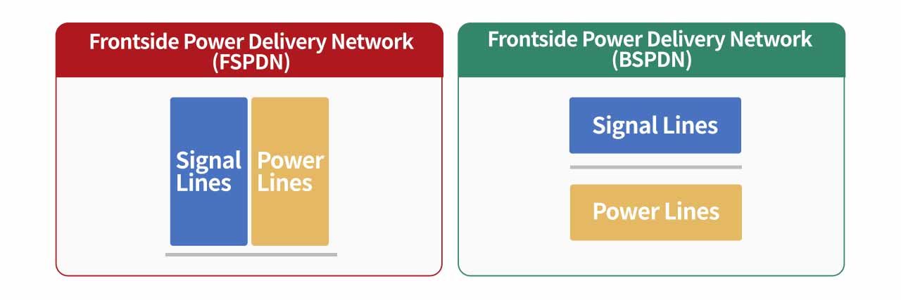
The mainstream approach today is frontside power delivery network (FSPDN). Current enters from the wafer’s front side and must pass through roughly 60–70 metal layers to reach the transistors at the bottom. Put simply, it’s like pulling a power cable from the top floor of a 70-story building down to the ground floor. As scaling continues and linewidths narrow, wire resistance increases, worsening IR drop. This also raises power consumption and interference risk—gradually turning power delivery into a major barrier to performance improvement.
In metal interconnect structures, routes can broadly be grouped into two types: One type is signal lines, which carry logic signals. Voltage and current are relatively small, but routing is complex and the count is enormous. The other type is power lines, whose main job is to bring external current into the transistors to provide the energy needed for switching.
However, under the traditional frontside power architecture, power lines must share the limited frontside routing area with a vast number of signal lines. As nodes shrink and metal layers increase, this competition for space shows up in several concrete engineering problems:
- As linewidths shrink, wire resistance rises, causing IR drop to keep worsening
- The effective voltage available at bottom-layer transistors becomes insufficient, and energy loss constrains achievable performance
- Power lines and signal lines sit too close together, increasing electromagnetic interference and further raising power and design complexity
Technology overview: what is backside power delivery network?
Backside power delivery moves the power-supply paths that were originally placed on the chip’s front side to the backside, freeing frontside routing capacity that would otherwise be consumed by both signal and power lines.
The foundation of backside power delivery relies on two key technologies: Buried Power Rail (BPR) and Nano Through-Silicon Via (n-TSV).
- Buried Power Rail (BPR): This embeds vertical power rails (VDD, VSS) directly into the substrate, so the power-delivery path no longer occupies the frontside metal interconnect stack. It also becomes fully separated from the back-end-of-line (BEOL) metal routing used for signal transmission. Structurally, this design “splits” power and signal into two systems, preventing them from competing for limited routing real estate.
- Nano Through-Silicon Via (n-TSV): This forms dense, nanoscale vertical vias in the substrate and fills them with conductive material, creating vertical conductive channels from the chip’s backside down to the transistor layer. With n-TSVs, power and ground can be fed directly from the backside, sharply shortening the delivery path and reducing resistance and IR drop.
In short, BPR provides a stable power backbone within the substrate, while n-TSVs serve as the crucial bridge connecting backside power to the front-end transistors—making “powering from the back” practical for advanced logic nodes.
TSMC Super Power Rail backside power delivery technology
Unlike Intel’s earlier PowerVia approach, TSMC’s backside power delivery technology is called Super Power Rail (SPR). TSMC uses a back-to-back approach—directly implementing backside power delivery—and it is also the most complex among the three currently known implementation paths.
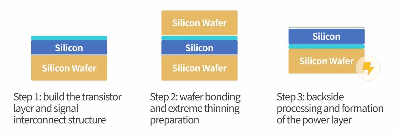
Step 1: build the transistor layer and signal interconnect structure
The process begins with a silicon wafer about 600,000 nm (600 µm) thick as the base. A transistor layer about 100 nm thick is built on top, followed by roughly 500 nm of signal interconnect. Unlike traditional flows, this stage only constructs signal routing—not power lines—because in a backside-power architecture, the power distribution network is implemented on the wafer backside, allowing the early metal stack to focus on signal transmission.
Step 2: wafer bonding and extreme thinning preparation
After the signal interconnect region is completed, the wafer is bonded to another silicon wafer (also about 600,000 nm thick) via wafer bonding, with the top wafer serving as a carrier wafer. This provides the mechanical support required for subsequent backside processing and extreme thinning. Since the original device wafer will be thinned from 600 µm down to essentially just the transistor layer, the structure would otherwise lose rigidity and could not withstand tool clamping, handling, or thermal and mechanical stress during later steps.
Step 3: backside processing and formation of the power layer
After bonding, the wafer enters grinding and chemical mechanical planarization (CMP), removing the original silicon substrate entirely and leaving only the transistor layer formed in the front-end steps. The wafer is flipped at this stage, with the original backside now facing up. Next, through silicon-via processing opens access below the transistors to create backside power channels, and a backside power metal layer about 500 nm thick is deposited—completing the backside power-delivery layer.
Key steps in backside power delivery: wafer thinning and reclaimed wafers
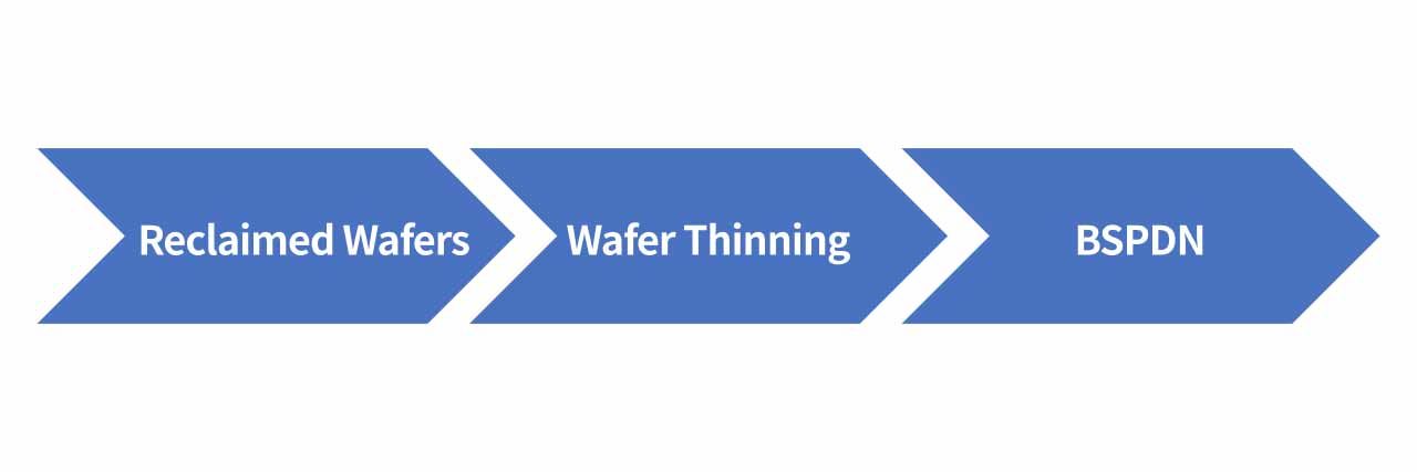
In backside power delivery and advanced packaging, wafer thinning is a critical step. Because the circuitry is fabricated on the wafer’s front side, front-end processes require a wafer with sufficient thickness and structural strength to survive high temperatures and many process steps. But once the circuitry is finished, keeping the wafer too thick limits backside power routing, thermal performance, and stacked packaging designs. Therefore, in practice the wafer is aggressively thinned from the backside after major processing is complete, to meet thickness and structural requirements for backside power and advanced packaging.
However, after thinning, the wafer becomes extremely fragile and can no longer tolerate later processing and handling. This makes wafer bonding a necessary prerequisite. By temporarily bonding the device wafer to a carrier wafer, the process gains the mechanical support needed to maintain stability and yield during thinning and backside processing.
In this flow, reclaimed wafers are widely used both as carrier wafers and as process test wafers. On one hand, a carrier wafer does not need product functionality—only flatness and mechanical strength—so reclaimed wafers can meet requirements and be reused. On the other hand, as bonding, thinning, and backside steps are introduced, process verification and tool calibration demand far more test wafers; reclaimed wafers help control costs.
Overall, wafer thinning determines feasibility, wafer bonding ensures process stability, and reclaimed wafers support volume production and cost structure—these three are tightly linked and all essential.
Reclaimed Wafers
A reclaimed wafer is a silicon wafer previously used in semiconductor manufacturing that remains structurally intact and is reprocessed—through film removal, grinding, CMP polishing, and defect inspection—for reuse in process monitoring, testing, or dummy-wafer applications. Because it is not used as a final product wafer, its cost is clearly lower than a prime wafer, while still meeting fabs’ needs for process stability and equipment calibration.
In backside power processes, reclaimed wafers are often used as carrier wafers. When the device wafer must be back-ground for electrical interconnection—thinned to around 100 µm, or even below 10 µm—its mechanical strength drops sharply, making it prone to breakage or severe warpage during handling or high-temperature steps. The carrier wafer’s key role is to provide a stable supporting base so the ultrathin device wafer can remain intact and complete subsequent lithography, metal deposition, CMP, and dry etch steps, while reducing yield loss caused by cracking or warpage. In advanced packaging and high-end AI chip manufacturing, carrier-process maturity has directly affected overall manufacturing cost, yield performance, and product stability.
Manufacturing flow
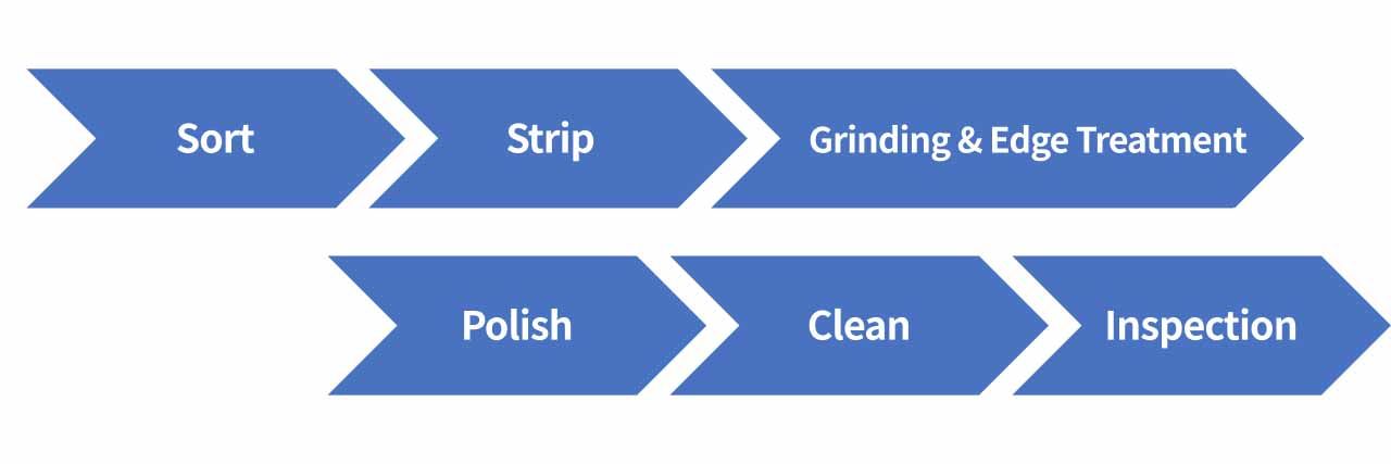
1. Sort The goal of this step is to screen out unsuitable wafers before reclamation starts, preventing metal contamination from entering the reclaim line. Incoming wafers are inspected one by one, including appearance defects, wafer type, and basic material/structural characteristics. The results determine whether a wafer is suitable and which reclaim recipe should be used.
2. Strip Stripping removes the various films on the wafer surface so it can enter subsequent reclaim steps. The method is adjusted based on incoming condition and is typically performed in automated wet batch cleaning systems. Common chemistries include SPM (sulfuric acid + hydrogen peroxide), high-concentration HF etch, and alkaline etch (such as KOH), selected and combined depending on film type. If metal films are present, additional pretreatment is required. The key is complete film removal while avoiding cross-contamination between wafers.
3. Grinding & edge treatment For SOI wafers with thicker structures and buried insulators, or when specific films must be removed, grinding is often performed first—along with edge treatment and edge rounding—to improve wafer shape and process stability. Grinding removes material quickly but is harder to control for thickness and surface uniformity, so CMP is applied afterward for smoothing and final polish to improve surface quality and flatness for downstream processes.
4. Polish Polishing can be single-side or double-side, combining chemical and mechanical action. Double-side polishing can reduce TTV (total thickness variation) and improve thickness consistency. After polishing, the wafer returns to a bare-silicon surface with overall thickness below the original. However, polishing can leave slurry residue, particles, or metal contamination, which must be thoroughly removed in later cleaning.
5. Clean Final cleaning is usually done in automated wet batch tools and can include multiple sequential cleaning steps in the same system. Standard RCA clean is used, including: SC-1 (H₂O / NH₄OH / H₂O₂): removes particles and residues SC-2 (H₂O / HCl / H₂O₂): reduces metal contamination After cleaning, surface metal concentration can be reduced to below 5×10¹⁰ atoms/cm², and in practice often below 1×10¹⁰. Surface-tension drying completes the flow.
6. Inspection After reclamation, wafers are graded by thickness and surface defect count. A typical spec for test wafers is fewer than 50 LPD (Light Point Defect) at 0.12 µm. Since test wafers are used for tool tuning and troubleshooting, defect control is critical because it directly affects diagnostic accuracy.
Advantages of reclaimed wafers
- Lower production cost: reclaimed wafers typically cost about 20–30% of new prime wafers, reducing spending for testing and non-critical process uses
- Lower carbon footprint and sustainability: compared with new wafer manufacturing, reclamation can reduce energy and water use by about 60–80%, aligning with emissions reduction and ESG goals in semiconductors
- Improved process stability and yield: extensive use of reclaimed wafers for validation and testing helps detect process drift early and reduce mass-production risk
Advanced nodes are driving higher demand for reclaimed wafers
As nodes keep shrinking, demand for reclaimed wafers rises noticeably. In earnings calls, Shengyang Semiconductor indicated:
- 5 nm: for 100,000 wafer starts, about 100,000 reclaimed wafers are needed
- 3 nm: reclaimed wafer demand increases to about 2.2×
- 2 nm: reclaimed wafer demand rises further to 2.6×+
This suggests that the more advanced the node, the greater the reliance on testing, calibration, and process control. Reclaimed wafers are no longer just auxiliary materials—they have become foundational resources supporting advanced-node operations. Historically, reclaimed wafers were merely testing consumables in front-end manufacturing. But as nodes advance and advanced packaging demand increases, their role has shifted toward supporting process stability, lowering cost, and enabling ultrathin device-wafer manufacturing.
Reclaimed wafers were originally just test consumables, but as scaling and advanced packaging accelerate, they have become foundational materials that help stabilize processes, reduce cost, and support ultrathin device wafer manufacturing.
Wafer thinning
Wafer thinning refers to removing material from the backside of a wafer after front-end processing, reducing overall wafer thickness. The purpose is to meet miniaturization and advanced packaging requirements—enabling thinner, smaller chips and supporting stacking and high-density integration for space-constrained electronics that still demand high performance.
Benefits of wafer thinning
Wafer thinning is not just about being thinner—it directly affects packaging and performance, including:
- Better thermal performance: thinner chips conduct heat more effectively, improving long-duration stability for high-performance devices
- Smaller package size: thinner dies support denser packaging and stacking, helping device miniaturization
- Lower internal stress: thick wafers can accumulate stress with temperature changes; thinning helps reduce cracking risk
- Improved electrical behavior: shorter structural distances can improve high-frequency signals and overall electrical efficiency
- Higher dicing and packaging yield: thinned wafers are less likely to chip or be damaged during dicing and packaging
Limits and challenges
Because ICs are built on the wafer front side, front-end processing requires high planarity and structural stability. Thinning can only occur after major processing and is achieved by gradually removing backside material. Planarity control becomes a key yield driver.
As nodes shrink, requirements for backside grinding uniformity and flatness become much stricter, increasing the importance of CMP. Diamond disks—critical consumables for conditioning grinding pads—directly determine the stability and consistency of grinding conditions. Their precision and durability affect thinning quality and final yield, making them indispensable in advanced processes.
Common wafer thinning methods
In practice, thinning is not done with a single method; fabs mix approaches based on process needs:
- Mechanical grinding: the most common method, typically including coarse and fine grinding
- Chemical mechanical polishing (CMP): combines slurry chemistry with mechanical action for improved flatness and surface quality, but with higher cost and tighter requirements
- Chemical etching: often used for surface finishing after grinding
- Plasma-related methods: use plasma/chemical reactions and can offer better thickness uniformity, commonly used in advanced processes
In TSMC’s backside power delivery flow, the primary methods are mechanical grinding and CMP. The core idea is to fabricate circuits on a thick wafer for process stability, then thin from the backside to meet product needs for miniaturization, thermal performance, and advanced packaging. As advanced packaging and high-performance chips evolve, wafer thinning has become an essential manufacturing step.
Backside power delivery comparison: TSMC vs. Intel vs. Samsung
The competitive landscape is becoming a three-way race. Beyond TSMC’s push into backside power delivery, Intel is trying to regain technology leadership by ramping commercial production earlier, while Samsung is following and targeting mass production in 2027. Although the overall goal is the same, implementation differs significantly—especially in power tap points and manufacturing complexity.
Adoption timelines
Intel PowerVia commercialization progress
Intel’s PowerVia is a key component of its Intel 18A process node, introduced alongside RibbonFET (GAA), aiming to reduce IR drop and free frontside routing resources through backside power delivery. At CES 2026, Intel officially unveiled Core Ultra Series 3 (Panther Lake), described as the first client processors adopting the 18A node—signaling PowerVia’s transition from R&D into a commercial product cycle.
In terms of maturity, 18A is still in ramp. Intel’s management has said current yields can support shipment, but the cost structure remains below the desired level, indicating backside power-related steps are still challenging for cost and yield management. In other words, PowerVia has entered commercial viability, but its long-term economics and full impact on PPA still need more high-volume data. Strategically, Intel also positions 18A and PowerVia as differentiators for its foundry services. While external customer volume-production cases have not been publicly disclosed, U.S.-based manufacturing provides strategic value in supply-chain security and policy-driven applications.
Samsung SF2Z roadmap
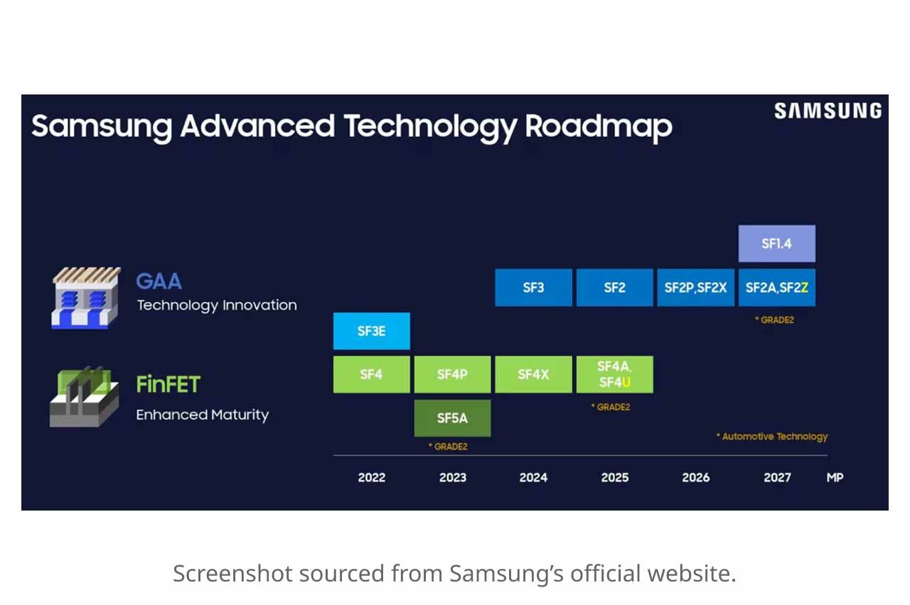
Samsung’s SF2Z is an enhanced version within its 2 nm family that integrates backside power delivery. It mainly targets HPC and AI applications, with mass production expected around 2027. SF2Z builds on Samsung’s MBCFET (GAA) platform, leveraging experience accumulated over multiple generations of nanosheet transistor manufacturing.
SF2Z aims to address power-delivery bottlenecks in high power-density designs and further improve overall PPA. However, Samsung has not yet released specific performance or power-reduction figures, so the realized benefits still need mass-production validation. Compared with peers, the key risk is later timing; whether SF2Z can offset schedule lag with sufficient PPA gains and yield performance will be critical to its competitiveness.
Key differences in Intel PowerVia’s manufacturing approach
Intel was the earliest to introduce backside power delivery, while TSMC’s route differs in several important ways:
PowerVia pre-embeds nano-TSVs in the front-end process
Unlike TSMC Super Power Rail, which forms power contacts directly from the backside, Intel PowerVia’s core design embeds nano-TSVs during front-end transistor fabrication. These nano-TSVs are created at the transistor stage but initially as “blind vias” that do not yet pass through the wafer. This differs clearly from packaging-level TSVs: their nanoscale dimensions and tight alignment with transistors allow vertical power connections in a very small footprint without consuming standard-cell layout area. In contrast, TSMC Super Power Rail does not use TSV-like structures, instead relying on backside metal to directly connect to transistor endpoints—reflecting different engineering philosophies for vertical power conduction.
PowerVia moves power entirely to the backside, letting frontside metals focus on signals
In PowerVia, Intel moves power and ground fully to the backside so that all frontside metal layers can focus on signal routing—unlike TSMC, which still retains part of the power structure on the front side. PowerVia therefore gains greater frontside signal-routing freedom, helping reduce detours, crosstalk, and RC delay—one reason Intel emphasizes benefits in logic density and clock scaling.
A key risk: thinning must precisely expose the embedded nano-TSVs
PowerVia also requires wafer flip, bonding to a carrier, and extreme thinning, but with a different risk profile. Because nano-TSVs are already embedded inside the wafer, thinning must stop precisely at the TSV tips to fully expose them without damage. This places extremely tight demands on thickness control and warpage management, making PowerVia’s yield and cost highly dependent on bonding and grinding accuracy. By contrast, TSMC Super Power Rail faces more challenges in backside alignment and direct contact to source/drain (S/D) regions—so the two have different risk structures.
PowerVia uses a three-stage power-delivery structure
On the wafer backside, Intel builds a dedicated coarse-pitch backside power grid and uses nano-TSVs to transmit power vertically to the transistor contact layer. This three-stage “backside power → TSV → transistor” structure is PowerVia’s defining feature, and contrasts with TSMC’s approach of backside metal directly contacting transistor endpoints. PowerVia’s advantage is a highly controllable vertical conduction path, at the cost of added process steps and structural complexity.
Overall comparison
As backside power delivery moves toward high-volume manufacturing, TSMC, Intel, and Samsung have chosen different routes, reflecting differences in process integration capability, risk tolerance, and node strategy:
- Intel introduced PowerVia at 18A first, emphasizing design continuity and manufacturability
- Samsung combines backside power with its buried power rail concept under a GAA platform, aiming to balance density and performance
- TSMC’s A16 Super Power Rail is viewed as the most forward-leaning option, with potentially the strongest scaling upside—but also higher process complexity and ramp challenges
The table below compares the three strategies across timing, transistor/power architecture, connection mechanisms, and performance/risk considerations to evaluate each player’s positioning in the next generation of advanced-node competition.
| Category | Super Power Rail | PowerVia | BSPDN |
|---|---|---|---|
| Company | TSMC | Intel | Samsung |
| Mass production timing | 2H26 | 2H25 | 2027 |
| Performance impact | 1) ~10% higher frequency at the same voltage 2) ~15%–20% lower power at the same frequency and design complexity 3) ~7%–10% higher transistor density | 1) Standard-cell utilization >90% in most chip areas 2) ~30% improvement in voltage droop 3) ~6% higher frequency | 1) ~14.8% lower wafer area utilization 2) ~9.2% shorter routing length, helping reduce resistance and improve current delivery |
| Technical highlights | 1) Introduced at A16 and combined with a GAA transistor architecture 2) Directly connects power lines to transistor source/drain (S/D), improving power-delivery efficiency | 1) Introduced at 18A and combined with RibbonFET 2) Uses nano-TSVs to connect the backside power network to the transistor contact layer | Introduced at SF2Z and combined with GAA (MBCFET) |
Impact: backside power delivery may reshape the supply chain
For the broader global semiconductor ecosystem around TSMC, the adoption of backside power delivery is not only a process breakthrough—it could also reshape market structure and supply-chain allocation over the coming years. The global semiconductor market is in a high-growth phase driven by AI demand, where advanced logic nodes and premium products such as HBM memory are key growth engines. This implies ongoing pressure to design and manufacture ultra-high-performance chips, and backside power architectures align well with that demand environment.
From a positioning perspective, TSMC’s move to introduce Super Power Rail as part of BSPDN at A16 is aimed at meeting increasingly demanding power integrity and energy-efficiency requirements for AI accelerators, HPC platforms, and cloud data centers—not merely shrinking linewidths for the sake of Moore’s Law. This strategy can offer customers better performance-per-watt and more design headroom for power integrity, especially for chips that integrate large compute blocks and high-bandwidth memory. SPR’s value may extend beyond single-die performance to enabling the system-level design requirements of high-end applications.
From a supply-chain standpoint, broad adoption of backside power delivery could drive structural upgrades across upstream and downstream segments. Demand for advanced equipment and materials is likely to rise in parallel—touching wafer thinning, backside bonding, high-precision inspection, and advanced packaging. Backside power delivery and reclaimed-wafer usage are also accelerating demand for process materials and equipment, including grinding consumables and carrier wafers—raising the value of these high-precision consumables. This means TSMC’s technology choices will influence not only its own manufacturing platform, but also spur incremental growth across relevant supply-chain categories.
In addition, amid global supply-chain competition and more diversified end-market demand, TSMC’s sustained lead in the most advanced nodes can reinforce its leadership in high-end logic and AI chip production, further strengthening customer alignment. As different applications require higher PPA and reliability, advanced backside power delivery may become a standard part of chip design. Foundries that can offer high-performance platforms will likely have stronger pricing and bargaining power. Under this demand-driven technology adoption, TSMC’s role as the world’s leading foundry could be further reinforced, with potential upside to its long-term revenue mix and market positioning.
Taiwan suppliers that may benefit from BSPDN
Kinik (1560.TW)
Kinik is an important supplier of CMP-related consumables in semiconductor manufacturing, focusing on precision grinding and planarization consumables needed for advanced nodes. Its products include diamond disks, grinding wheels, and reclaimed wafers, and they are mainly used by leading foundries such as TSMC. The company began with traditional grinding wheels, and after acquiring key diamond-disk capabilities—and aligning with TSMC’s supply-chain localization strategy—successfully transformed into a precision consumables manufacturer with core grinding and cutting competencies. Its competitive edge lies in diamond disks being critical CMP consumables with low substitutability and high qualification barriers, plus long-term deep collaboration with TSMC. It is estimated to hold about ~70% share in 3 nm diamond-disk supply and also has integrated capabilities spanning diamond disks and reclaimed wafers.
Under the BSPDN trend, Kinik could benefit from:
- Structurally resilient demand for diamond disks; as 2 nm mass production advances and flatness requirements tighten, monthly shipments have exceeded 50,000 units
- Rising reclaimed-wafer demand driven by advanced-node R&D, as more process validation and tool calibration support steady growth momentum
Overall, Kinik holds a strong position as a key diamond-disk supplier within TSMC’s supply chain and also has advantages in reclaimed wafer manufacturing—making it one of the core beneficiaries tied to TSMC’s advanced-node demand.
Phoenix Silicon (8028.TW)
Shengyang Semiconductor is a Taiwan-based wafer-material provider with long-standing expertise in reclaimed wafers and wafer-thinning processes, focusing on advanced-node and high-end manufacturing needs. Its core businesses include reclaimed wafer supply, wafer thinning, and related material-processing technologies, serving major customers such as TSMC. Key strengths include long-term collaboration with TSMC that builds process understanding and customer stickiness, as well as high market share and scaled mass-production capability in reclaimed wafers.
Under the BSPDN trend, Shengyang may benefit from:
- Continued node advancement raising tool calibration and process test demand, driving higher reclaimed wafer usage
- Extreme thinning and backside processing requiring temporary bonding for mechanical support, increasing carrier-wafer demand in parallel
Overall, Shengyang’s strong market position in reclaimed wafers and deep participation in TSMC’s advanced-process supply chain—together with increased carrier-wafer demand driven by backside power delivery—make it one of the key beneficiaries of related process and material growth.
Skytech (6937.TW)
Skytech is Taiwan’s first local equipment maker with mass-production capability for advanced semiconductor tools. Its products include PVD, ALD, and wafer bonding/debonding equipment, serving semiconductor and compound-semiconductor manufacturing. ALD, in particular, is considered critical for high-precision backside metal and dielectric deposition. Its competitive advantage is being one of the few Taiwanese suppliers able to mass-produce advanced front-end tools, supported by solid R&D. Its equipment portfolio extends from PVD and ALD into wafer bonding and debonding—forming a relatively complete front-end tool lineup—and it can respond quickly and precisely to customer needs, maintaining a pace of roughly one new tool introduction per year.
Under the BSPDN trend, Skytech may benefit from:
- The continuing push for localization of advanced front-end equipment, as one of the few domestic suppliers capable of directly providing such tools
- More demand for temporary bonding and debonding equipment as backside power delivery is introduced, expanding the application space for its related tools
Overall, Skytech is one of the few Taiwanese suppliers capable of mass-producing advanced front-end equipment, with products spanning ALD and PVD and deep relevance to advanced nodes and backside power processes. It stands to benefit from higher demand for temporary bonding/debonding tools under the localization trend.
