Overview of the Semiconductor Packaging Industry
The wafer production process encompasses design, front-end fabrication, and back-end assembly and testing (OSAT), with packaging being an essential step after wafer fabrication. Bare dies cannot be directly utilized after wafer foundry processes—they must go through packaging and testing before becoming final products ready for shipment.
The core objectives of packaging are threefold:
- Mechanical and environmental protection to prevent damage from moisture, oxidation, and external stress.
- Stable electrical connections and signal transmission, using bumps, wire bonding, substrates, or fan-out structures to integrate chips into PCBs and systems.
- Thermal dissipation and power management, which are critical for high-power CPUs, GPUs, and ASICs due to their sensitivity to heat and power delivery—making packaging a key factor in performance and reliability.
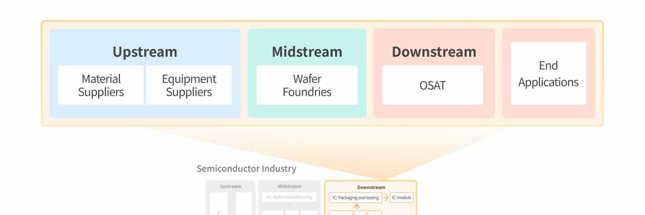
Industry Supply Chain
The packaging process is not handled by packaging houses alone—it requires close collaboration across the supply chain to produce high-yield and reliable chips. This ecosystem includes upstream equipment and material suppliers, midstream wafer foundries, downstream OSAT providers, and various end-application vendors, all interconnected to support the advancement of semiconductor processes and packaging technologies.
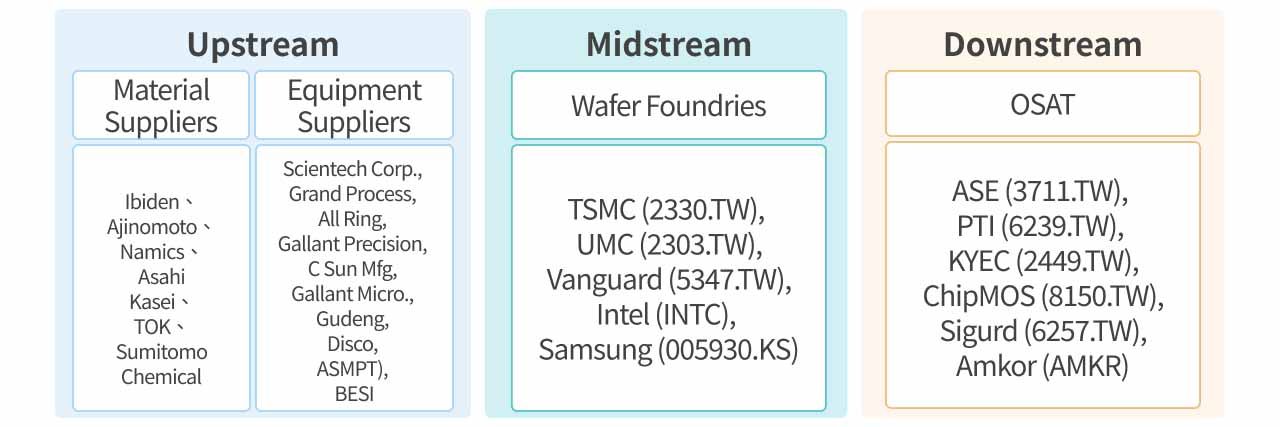
| Upstream | Midstream | Downstream | End Applications | |
|---|---|---|---|---|
| Material Suppliers | Equipment Suppliers | Wafer Foundries | OSAT | |
| Ibiden (4062.T), Ajinomoto (2802.T), Namics (4783.T), Asahi Kasei (3407.T), TOK (4186.T), Sumitomo Chemical (4005.T) | Scientech Corp. (3583.TW), Grand Process (3131.TW), All Ring (6187.TW), Gallant Precision (5443.TW), C Sun Mfg (2467.TW), Gallant Micro. (6640.TW), Gudeng (3680.TW), Disco (6146.T), ASMPT (0522.HK), BESI (BESI.AS) | TSMC (2330.TW), UMC (2303.TW), Vanguard (5347.TW), Intel (INTC), Samsung (005930.KS) | ASE (3711.TW), PTI (6239.TW), KYEC (2449.TW), ChipMOS (8150.TW), Sigurd (6257.TW), Amkor (AMKR) | AI, Automotive, Industrial Control, Networking, Memory, Cloud, Consumer Electronics |
Upstream: Packaging Materials Suppliers
Japanese Players Dominate the Market
Positioned upstream in the packaging supply chain, materials suppliers directly impact chip heat dissipation, reliability, and final form factor. Materials are typically categorized into substrates, lead frames, encapsulants/resins, bonding wires, and various process chemicals. Among these, substrates represent the highest value and greatest technical barrier—especially in AI and high-performance computing (HPC) where they are often bottlenecks.
The global packaging materials market is long dominated by Japanese suppliers, particularly in raw materials for advanced and wafer-level packaging. For example, Asahi Kasei holds over 50% of the market for photosensitive polyimide, which offers both electrical insulation and stress buffering. Ibiden, Ajinomoto, and Sumitomo Bakelite also lead in substrate, resin, and other material categories.
In contrast, Taiwan boasts strong high-volume manufacturing capabilities in IC substrates and lead frames, forming tight clusters with foundries and OSATs to enhance supply chain efficiency and competitiveness.
Highly Concentrated Global Equipment Market
Packaging equipment providers are also upstream, delivering critical tools used by wafer fabs and OSAT companies. These tools span wafer preparation, bonding, and package molding—especially those involved in 2.5D/3D advanced packaging and panel-level packaging, which represent the highest technological barriers. As advanced packaging becomes more widespread, these tools have evolved from relatively low-complexity back-end tools into critical enablers of Moore’s Law.
The global equipment market is highly concentrated. Japan’s DISCO holds over 70% market share in wafer dicing and thinning, dominating chip thinning and separation processes. Netherlands-based BESI, Japan’s Advantest, and Towa lead in hybrid bonding, automated testing, and molding respectively. With growing demand for multi-chip and high-bandwidth applications, these firms are moving into high-power packaging and system-level testing, leveraging product upgrades and higher ASPs to benefit from AI server and HPC growth.
Taiwanese Equipment Firms Capitalize on Localization
Taiwanese players are known for modular and customized equipment solutions. Thanks to TSMC’s global leadership in advanced nodes and packaging, many local firms co-develop processes with TSMC and top OSATs, successfully integrating into the packaging supply chain. Localized supply, quick production ramp-up, and high customization allow Taiwanese vendors to build differentiation and maintain sustainable growth momentum.
Midstream: Wafer Foundries’ Business Models Are Evolving
Wafer foundries are responsible for fabricating wafers, which are then passed on to OSATs for packaging. Vanguard and PSMC are examples of players focused on front-end processes. However, as advanced nodes progress, traditional packaging is no longer sufficient for the precision, interconnect density, and thermal demands of high-end chips. Thus, leading-edge foundries are increasingly adopting integrated “fab + packaging” models. TSMC, Samsung, and Intel exemplify this trend, building in-house advanced packaging capabilities to ensure seamless front-end and back-end integration—critical for AI, HPC, and high-speed computing.
In the global foundry market, TSMC maintains a dominant lead, driven by deep expertise in advanced process technologies, high production yields, and a reliable supply chain. With over 70% market share in advanced nodes, TSMC is now judged not just on yield and cost but also its ability to support mass production of complex products. Its stability, client trust, and experience place it in an unshakable leadership position.
Mid to Downstream: OSAT Providers
Benefiting from TSMC’s Ecosystem, Mature Nodes Moving Toward One-Stop Services

OSAT companies handle packaging and testing post-wafer fabrication. Packaging includes legacy techniques, advanced packaging for AI/HPC and high-speed communication, and various stages of testing—from wafer probing to final and system-level testing. Advanced packaging supporting large GPUs, AI ASICs, and HBM stacking involves the highest technical thresholds.
OSAT business models fall into two types:
- Collaborating with foundries in advanced packaging (e.g., handling parts of TSMC’s CoWoS process) and offering their own packaging for peripheral AI chips or non-flagship AI GPUs;
- Providing full turnkey services including both packaging and testing—common for mature nodes—helping clients accelerate time-to-market and improve supply chain efficiency.
Taiwanese OSATs offer clear advantages in efficiency and customization. ASE, PTI, and KYEC lead in advanced packaging, memory packaging, and high-end testing respectively. Coupled with Taiwan's local ecosystem—testing interfaces, substrates, and materials—these firms deliver rapid development cycles, high yields, and integrated services, making them essential nodes in the global AI and HPC semiconductor supply chain.
Industry Outlook
Mature-Node Packaging is Cyclical; Gradual Recovery Expected in 2026
Chips completed through OSAT processes enter various end-use applications. Those made on nodes above 7nm are typically used in industrial, memory, and consumer electronics—sectors subject to cyclical demand. As such, mature-node packaging sees similar cycles.
UMC and Vanguard benefited from surging demand and tight capacity during the pandemic. But post-pandemic, with weak consumer demand and elevated inventories, plus pricing pressure from low-cost Chinese peers, the mature-node segment has been in decline since 2023. Weak 2025 recovery in smartphones and PCs continues to weigh on results. However, Taiwanese supply chain firms are signaling an upturn, suggesting the bottom is past and a gradual recovery starting in 2026.
Advanced Packaging Capacity Fully Booked; TSMC Establishes a Monopoly
Advanced packaging is driven by AI, HPC, and high-speed communication, where heterogeneous integration boosts overall performance. With growing chip sizes and power in AI and HPC, requirements for high bandwidth, low latency, and power efficiency are intensifying, making 2.5D/3D packaging and HBM stacking critical technologies. With NVIDIA, AMD, and major cloud providers scaling up AI chip orders, advanced packaging demand is structurally rising.
On the supply side, TSMC, Samsung, and Intel offer integrated front- and back-end solutions, while ASE and PTI represent leading OSAT providers. TSMC stands out with unmatched maturity in process and packaging integration, supply chain reliability, and yield. Its advanced packaging solutions are currently irreplaceable. In contrast, OSATs primarily collaborate with foundries and target peripheral AI chips, not core flagship GPUs.
Intel’s 2.5D EMIB remains mainly used for its own CPUs, with limited external adoption. Its 3D Foveros Direct technology is also mostly internal. Samsung’s 2.5D I-Cube/H-Cube and 3D X-Cube platforms have yet to secure key customers or scale.
In short, advanced packaging is now a foundational enabler of AI and HPC. Demand is surging, while supply is limited by high barriers and long lead times. TSMC’s depth in process-packaging integration, yield stability, and client stickiness gives it a dominant, defensible position.
OSATs Diversifying Advanced Packaging, but Revenue Contribution Remains Modest
TSMC remains the global leader, but other alternatives are gaining traction—especially from OSATs:
- ASE FOCoS (Fan-Out Chip-on-Substrate): Uses panel-level fan-out to package large chiplets with dense RDL on a square substrate. It improves area utilization and lowers costs, making it a potential CoWoS substitute in specific applications. ASE is ahead in commercialization due to early entry and volume experience.
- PTI FOPLP (Fan-Out Panel Level Packaging): Similar to TSMC’s InFO but uses glass as interposer—offering better area efficiency, thermal performance, lower warpage, and cost. It targets mid-to-high-end SoCs and AI peripheral chips and is expected to begin contributing revenue in 2026.
Other approaches such as Intel’s EMIB and Innolux’s PLP are also being watched. However, due to the lack of maturity, customer adoption, and scale, these solutions will have limited short-term impact but merit future monitoring.
Key Taiwanese Stocks to Watch
Taiwan’s advanced packaging growth will continue to be led by TSMC, primarily through CoWoS capacity expansion, with WMCM and SoIC also scaling up. Investors should prioritize TSMC and its core suppliers across all three platforms.
TSMC (2330.TW)
TSMC is the world’s leading dedicated foundry with major facilities in Taiwan, China, Japan, Germany, and the US. In Q3 2025, HPC and smartphones accounted for 57% and 30% of revenue, reflecting TSMC’s vital role in AI server CPUs/GPUs, networking chips, and flagship mobile SoCs. Advanced nodes (5nm and 3nm) now contribute over 60% of revenue.
Outlook for 2026:
- Tight advanced node capacity will enhance pricing power—TSMC plans a 3–8% hike for 3nm/2nm.
- N2 (2nm) ramp will yield >10% of revenue in its first year—higher than N5 (8%) and N3 (6%).
- Structural expansion of 3D Fabric platform—CoWoS capacity projected at 70k/120k/140k wafers per month by end-2025/26/27, growing 112%/71%/19% YoY, alongside SoIC/WMCM scaling from 2026.
With over 50% of revenue from AI/HPC, TSMC’s strong execution and long-term targets (20% CAGR, >53% gross margin, >25% ROE) support sustained growth in a data-driven world.
Grand Process Technology (3131.TW)
Grand Process Technology is a leading Taiwanese wet-process equipment provider focused on advanced packaging and wafer back-end. It supplies key equipment for CoWoS, SoIC, and WMCM, along with integrated chemical solutions.
It is a core TSMC supplier, has entered ASE’s advanced lines, and supports HBM-related capacity for key memory clients.
Growth drivers for 2026:
- TSMC/ASE capex for advanced packaging to grow 29% annually—driving demand for Grand Plastic’s wet-process equipment;
- Integrated hardware-chemical model enhances revenue and margins;
- Expansions at TSMC’s Taichung AP5, Zhunan AP6, Chiayi, and Tainan facilities, plus memory client orders into 2025–26 and new contributions from its high-margin subsidiary Tianhong.
Overall, Grand Process Technology is poised for strong revenue and profit growth through 2026, cementing its role as a key global supplier in advanced packaging equipment.
